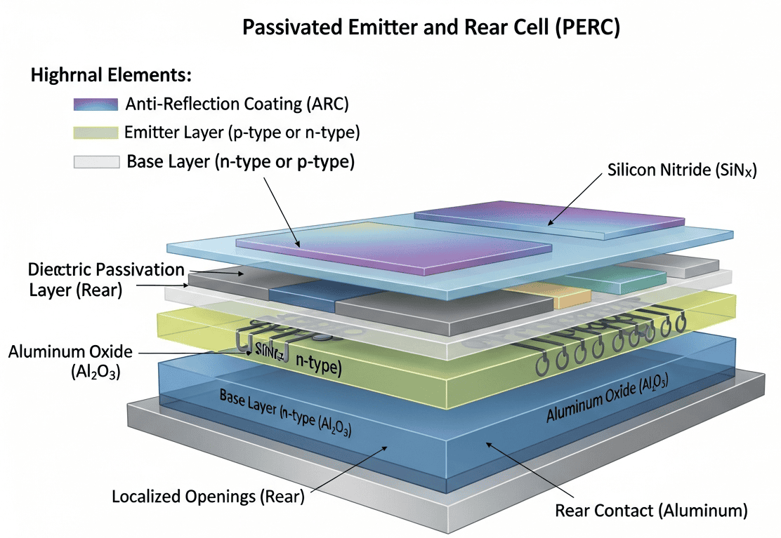

Passivated Emitter and Rear Cell (PERC) technology extends conventional aluminum back-surface-field solar cells by introducing a dielectric passivation layer — typically Al2O3 capped with SiNx — at the rear silicon surface, suppressing recombination and enhancing internal rear reflectance. Performance gains derive from reduced surface recombination velocity, improved minority carrier lifetime, and optimized local rear contacts opened via laser ablation.
Process integration addresses PECVD or ALD deposition uniformity, screen-printed metallization, firing profiles, and hydrogen passivation dynamics. Light-induced degradation from boron-oxygen defects and its mitigation through regeneration annealing remains an active research focus.
This page aggregates the latest peer-reviewed publications and granted patents spanning PERC cell physics, fabrication processes, bifacial variants, and module-level integration:
This is our latest selection of worldwide publications and patents in english on Passivated Emitter and Rear Cell (PERC), between many scientific online journals, classified and focused on Rear surface passivation, aluminum oxide passivation, silicon nitride passivation, local rear contact, laser contact opening, dielectric passivation layer, surface recombination velocity, minority carrier lifetime, rear reflectance, internal quantum efficiency, bifacial PERC, PERC+, rear emitter, front surface field, selective emitter, hydrogen passivation, firing process, Al2O3 deposition, PECVD deposition, ALD deposition, rear laser ablation, contact resistance, fill factor optimization, light-induced degradation, boron-oxygen defect, regeneration annealing, gettering process, bulk defect passivation, open-circuit voltage enhancement, screen-printed metallization and Passivated Emitter and Rear Cell.
Material-specific lighting requirements and contemporary illumination strategies for galleries
Published on 2026-07-08 by @OXFORD
Abstract: AbstractMuseum lighting simultaneously governs visual presentation and light-induced degradation of artworks. With the widespread adoption of light emitting diode technologies, traditional illuminance- and dose-based standards are increasingly insufficient to address the heterogeneous photochemical responses of different materials. This review synthesizes recent research on material-specific lighting requirements and contemporary illumination strategies for galleries, focusing on spectral power [...]
Our summary: This review addresses material-specific lighting needs and modern strategies for gallery illumination. It highlights the varying sensitivity of artworks to different light wavelengths and the impact on visual presentation and degradation. Optimized lighting approaches can significantly enhance energy efficiency while preserving artwork integrity.
museum lighting, photochemical responses, illumination strategies, energy optimization
Publication
Germanium-rich metal contact layers for pmos source and drain contacts
Patent published on the 2026-07-01 in EP under Ref EP4770328 by INTEL CORP [US] (Metz Matthew V [us], Dewey Gilbert [us], Karpov Ilya V [us], Sen Gupta Arnab [us], Budrevich Aaron A [us])
Abstract: [0001] Outdiffusion of germanium from silicon-germanium source and drain regions of PMOS (p-channel metal-oxide-semiconductor) field effect transistors into metal contact layers located on the PMOS source and drain regions can reduce the concentration of germanium layer in the silicon-germanium in the vicinity of the silicon-germanium layer-metal contact layer interface. This region of reduced germanium concentration can increase the parasitic contact resistance, which can have a deleterious eff[...]
Our summary: Germanium outdiffusion from silicon-germanium regions can degrade PMOS transistor performance. Adding germanium to metal contact layers mitigates this issue. This approach helps maintain germanium concentration and reduces parasitic contact resistance.
Germanium, PMOS, contact resistance, outdiffusion
Patent
Female terminal
Patent published on the 2026-06-18 in WO under Ref WO2026126903 by AUTONETWORKS TECH LTD [JP] (Kobayashi Shingo [jp])
Abstract: Disclosed is a female terminal capable of reducing contact resistance by suppressing excessive deflection of a deflection part while maintaining deflection property for absorbing a positional deviation between a male terminal and a contact part. A female terminal is composed of a pair of metal flat sheets. Each of the metal flat sheets has: a contact part that comes into contact with a male terminal; a connection part that is connected to another conductive member; a deflection part that allow[...]
Our summary: The female terminal reduces contact resistance by minimizing excessive deflection while allowing for positional deviation. It consists of metal flat sheets with contact and connection parts, and a deflection part for relative displacement. Displacement suppression protrusions prevent excessive movement between the male and female terminals during connection.
female terminal, contact resistance, deflection part, conductive connection
Patent
Integrated processing device
Patent published on the 2026-06-18 in WO under Ref WO2026127186 by IUCF HYU INDUSTRY UNIV COOPERATION FOUNDATION HANYANG UNIV [KR] (Park Jin Seong [kr], Song Yun Heub [kr])
Abstract: Disclosed is an integrated processing device integrating a deposition process for forming semiconductor patterns and removal of an oxide film. According to embodiments, an integrated processing apparatus may be implemented with a structure which includes a deposition and etching unit that performs a chemical vapor deposition (CVD)-based deposition process, an atomic layer deposition (ALD)-based deposition process, and an atomic layer etching (ALE) process, a structure which includes, separate fr[...]
Our summary: The integrated processing device combines deposition and etching processes for semiconductor pattern formation. It features units for chemical vapor deposition (CVD), atomic layer deposition (ALD), and atomic layer etching (ALE). The apparatus can be structured with separate or combined units for efficient processing.
integrated processing device, semiconductor patterns, chemical vapor deposition, atomic layer etching
Patent
Electrical connection plate, terminal post extension member, battery cell member and battery assembly
Patent published on the 2026-06-18 in WO under Ref WO2026124357 by D AUS ENERGY STORAGE TECH XIAN CO LTD [CN] (Chen Mengqi [cn], Lei Zhengjun [cn])
Abstract: The present invention belongs to the field of batteries, and specifically relates to an electrical connection plate, a terminal post extension member, a battery cell member and a battery assembly, which overcome the problems of poor connection stability, low electrical conductivity, etc., in existing electrical connections. The electrical connection plate comprises an electrical connection portion, wherein the electrical connection portion is provided with first welding portions, the first weldi[...]
Our summary: The invention includes an electrical connection plate, terminal post extension member, and battery cell member to enhance connection stability and conductivity. It features first and second welding portions that form seams for effective electrical connections. The design reduces contact resistance and improves electrical conduction efficiency in battery assemblies.
electrical connection, battery assembly, welding portions, conductivity
Patent
Thermoelectric conversion member, production method for same, and thermoelectric conversion element
Patent published on the 2026-05-28 in WO under Ref WO2026110560 by NATIONAL INST FOR MATERIALS SCIENCE [JP] (Mori Takao [jp], Li Airan [jp])
Abstract: The present invention provides: a thermoelectric conversion member that makes it possible to reduce contact resistance between a MgAgSb-based thermoelectric material and an electrode; a production method for the same; and a thermoelectric conversion element. A thermoelectric conversion member according to the present invention comprises at least: a thermoelectric conversion layer which comprises a p-type thermoelectric material that includes magnesium (Mg), silver (Ag), and antimony (Sb); and [...]
Our summary: The invention presents a thermoelectric conversion member that reduces contact resistance between a MgAgSb-based material and an electrode. It includes a p-type thermoelectric layer and an Sb layer on its end surface. The production method involves forming and sintering a laminate of raw materials for the thermoelectric material and the Sb layer.
thermoelectric conversion, contact resistance, production method, MgAgSb
Patent
Photovoltaic cell preparation method and photovoltaic cell
Patent published on the 2026-05-27 in EP under Ref EP4750273 by ZHEJIANG JINKO SOLAR CO LTD [CN] (Zeng Xianhuan [cn], Wang Yilan [cn], Li Chao [cn], Zhang Ning [cn])
Abstract: The present disclosure relates to a photovoltaic cell preparation method, and a photovoltaic cell. The method includes: preparing a substrate including a first surface and a second surface opposite to each other, wherein the first surface is a textured structure; placing the substrate into an ALD deposition chamber; sequentially depositing an aluminum-silicon layer and an alumina layer on the first surface; placing the substrate having the aluminum-silicon layer and the alumina layer into a PECV[...]
Our summary: The disclosure presents a method for preparing photovoltaic cells. It involves depositing aluminum-silicon and alumina layers, followed by a silicon nitride layer using PECVD. This process enhances the cell s efficiency by reducing damage from ultraviolet light through improved chemical bonding.
Photovoltaic cell, ALD deposition, PECVD deposition, conversion efficiency
Patent
External control of photocleavage reactivity in polymer networks to reconcile photodegradability and photostability
Published on 2026-04-13 by Hiroshi Masai @NATURE
Abstract: Polymer Journal, Published online: 13 April 2026; doi:10.1038/s41428-026-01165-6This review summarizes our recent strategies for controlling the photostability and photoreactivity of polymer materials. Beyond conventional photoreactive polymers, we have developed polymer systems that exhibit cooperative reactions triggered by combined light and acid stimuli, as well as tunable photoreactivity based on reversible intramolecular isomerization. These systems show significant promise for a wide rang[...]
Our summary: This review discusses strategies for controlling the photostability and photoreactivity of polymer materials. It highlights the development of polymer systems that respond to combined light and acid stimuli. The findings suggest potential applications in light-induced degradation and processing in light-irradiated environments.
photocleavage, photostability, polymer networks, photoreactivity
Publication