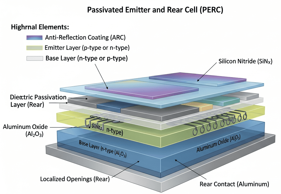

钝化发射极和背接触(PERC)技术通过在背面硅表面引入介电钝化层(通常为覆盖有SiNx的Al2O3),扩展了传统的铝背表面场太阳能电池,从而抑制复合并提高内部背面反射率。性能提升源于表面复合速度的降低、少数载流子寿命的延长以及通过激光烧蚀形成的优化局部背面接触。
工艺集成旨在解决PECVD或ALD沉积均匀性、丝网印刷金属化、烧结曲线和氢钝化动力学等问题。光致硼氧缺陷引起的性能退化及其通过再生退火的缓解仍然是当前研究的热点。
本页面汇总了最新的同行评审出版物和已授权专利,内容涵盖 PERC 电池物理、制造工艺、双面变体和组件级集成:
这是我们最新精选的全球英文出版物和专利,涵盖钝化发射极和背接触 (PERC) 的众多科学在线期刊,并按以下主题进行分类和重点介绍:背面钝化、氧化铝钝化、氮化硅钝化、局部背接触、激光接触开口、介电钝化层、表面复合速度、少数载流子寿命、背面反射率、内部量子效率、双面 PERC、PERC+、背发射极、正面场、选择性发射极、氢钝化、烧结工艺、Al2O3 沉积、PECVD 沉积、ALD 沉积、背面激光烧蚀、接触电阻、填充因子优化、光致退化、硼氧缺陷、再生退火、吸杂工艺、体缺陷钝化、开路电压增强、丝网印刷金属化以及钝化发射极和背接触。
Rechargeable battery and battery pack including the same
Patent published on the 2026-10-07 in EP under Ref EP4819300 by SAMSUNG SDI CO LTD [KR] (Seong Yeon Kyeong [kr], Kim Hyun [kr])
Abstract: A battery and a battery pack including the same are disclosed. A battery of a battery pack having a cooling member includes an electrode assembly and a case in which the electrode assembly is accommodated, and a thermal contact resistance between the case and the electrode assembly in a first portion of the battery adjacent to the cooling member is greater than a thermal contact resistance between the case and the electrode assembly in a second portion of the battery that is farther from the coo[...]
Our summary: The content describes a rechargeable battery and battery pack with a cooling member. It highlights the thermal contact resistance differences between two portions of the battery. The design aims to improve thermal management in the battery system.
Rechargeable battery, battery pack, cooling member, thermal contact resistance
Patent
Ultrahigh bandgap algan channel hemts with low contact resistance
Patent published on the 2026-10-01 in US under Ref US20260303761 by WISCONSIN ALUMNI RES FOUND [US] (Pasayat Shubhra S [us], Mukhopadhyay Swarnav [us], Gupta Chirag [us], Gohel Khush [us])
Abstract: Aluminum gallium nitride (AlGaN) channel high electron mobility transistors (HEMTs), methods of operating the AlGaN HEMTs, and methods of making the AlGaN HEMTs are provided. The AlGaN HEMTs include source and drain contacts on a highly n-type doped, reverse graded AlGaN contact layer. At least a portion of the HEMT heterostructure is partially or fully strained relaxed to provide low contact resistance at the interface between the contact layer and the source and/or drain contact.[...]
Our summary: The content discusses ultrahigh bandgap AlGaN channel HEMTs with low contact resistance. It details methods for operating and fabricating these transistors. The HEMTs feature a reverse graded AlGaN contact layer with n-type doping and a strained relaxed heterostructure.
AlGaN, HEMTs, contact resistance, heterostructure
Patent
Tungsten-modified nickel-alumina composite catalyst prepared through one-pot firing process
Patent published on the 2026-10-01 in WO under Ref WO2026205711 by UNIV ULSAN FOUND IND COOP [KR] (Shin Eun Woo [kr], Jamsaz Azam [kr])
Abstract: The present invention relates to a catalyst manufacturing method in which a tungsten-modified nickel-alumina composite catalyst prepared through a one-pot firing process is charged into a reactor and subjected to an in-situ reduction treatment. According to the present invention, the addition of tungsten suppresses coke formation, and thus catalytic activity is excellent and persists without degrading even after a long reaction time.[...]
Our summary: The invention describes a method for manufacturing a tungsten-modified nickel-alumina composite catalyst using a one-pot firing process. This catalyst undergoes in-situ reduction treatment in a reactor. The addition of tungsten enhances catalytic activity and prevents coke formation, ensuring durability over extended reaction times.
Tungsten, nickel-alumina, composite catalyst, one-pot firing
Patent
Display device
Patent published on the 2026-09-24 in US under Ref US20260293397 by LG DISPLAY CO LTD [KR] (Na Hyunseok [kr], Kim Woosung [kr], Cho Seongsoo [kr], Shin Sanghak [kr])
Abstract: A display device includes a substrate having transistors and lower connection electrodes, insulating and protective layers disposed on the substrate, and an element disposed above an adhesive layer. An upper connection electrode has a concave end portion that laterally contacts side surfaces of an element contact electrode while also electrically connecting to a lower connection electrode through the adhesive layer. A further upper electrode connects another element contact electrode to an upper[...]
Our summary: A display device consists of a substrate with transistors and connection electrodes. It features a structure that maintains electrical coupling despite alignment variations. This design enhances contact area, reduces resistance, and simplifies assembly while lowering power consumption.
display device, transistors, electrical stability, power consumption
Patent
Ultrathin aluminum-rich capping layers for improving internal quantum efficiency in ultraviolet leds
Patent published on the 2026-09-03 in WO under Ref WO2026183559 by THE REGENTS OF THE UNIV OF CALIFORIA [US] (Wang Michael [us], Gong Wenting [us], Nakamura Shuji [us], Speck James S [us])
Abstract: With the use of ultrathin aluminum-rich capping layers, the efficiency of ultraviolet (UV) or far-UV light-emitting diodes (LEDs), laser diode (LDs), or other light-emitting devices is improved through the reduction of carrier loss due to electron overshoot and improved radiative efficiency through improved quantum confinement.[...]
Our summary: Ultrathin aluminum-rich capping layers enhance the internal quantum efficiency of ultraviolet LEDs. They reduce carrier loss caused by electron overshoot. Improved quantum confinement leads to better radiative efficiency in light-emitting devices.
Ultrathin layers, aluminum-rich, quantum efficiency, ultraviolet LEDs
Patent
Method for manufacturing electronic device board connector
Patent published on the 2026-08-13 in WO under Ref WO2026168639 by GTG SOLUTION CO LTD [KR] (Lim Jong-gae [kr])
Abstract: The present invention relates to a method for manufacturing an electronic device board connector. The objective of the present invention is to quickly and accurately manufacture a board connector, which has a connection pin, a spring part and a solder terminal integrally formed to have a constant contact resistance while not causing a connection resistance and not being affected by usage time. The present invention relates to the method for manufacturing an electronic device board connector, com[...]
Our summary: The invention describes a method for manufacturing an electronic device board connector. It includes a spring bending process, a connection pin compression binding process, and a spring-part matching and bending process. The goal is to create a connector with low contact resistance and high durability.
connector manufacturing, electronic device, spring bending process, connection pin
Patent
Material-specific lighting requirements and contemporary illumination strategies for galleries
Published on 2026-07-08 by @OXFORD
Abstract: AbstractMuseum lighting simultaneously governs visual presentation and light-induced degradation of artworks. With the widespread adoption of light emitting diode technologies, traditional illuminance- and dose-based standards are increasingly insufficient to address the heterogeneous photochemical responses of different materials. This review synthesizes recent research on material-specific lighting requirements and contemporary illumination strategies for galleries, focusing on spectral power [...]
Our summary: This review addresses material-specific lighting needs and modern strategies for gallery illumination. It highlights the varying sensitivity of artworks to different light wavelengths and the impact on visual presentation and degradation. Optimized lighting approaches can significantly enhance energy efficiency while preserving artwork integrity.
museum lighting, photochemical responses, illumination strategies, energy optimization
External control of photocleavage reactivity in polymer networks to reconcile photodegradability and photostability
Published on 2026-04-13 by Hiroshi Masai @NATURE
Abstract: Polymer Journal, Published online: 13 April 2026; doi:10.1038/s41428-026-01165-6This review summarizes our recent strategies for controlling the photostability and photoreactivity of polymer materials. Beyond conventional photoreactive polymers, we have developed polymer systems that exhibit cooperative reactions triggered by combined light and acid stimuli, as well as tunable photoreactivity based on reversible intramolecular isomerization. These systems show significant promise for a wide rang[...]
Our summary: This review discusses strategies for controlling the photostability and photoreactivity of polymer materials. It highlights the development of polymer systems that respond to combined light and acid stimuli. The findings suggest potential applications in light-induced degradation and processing in light-irradiated environments.
photocleavage, photostability, polymer networks, photoreactivity
Publication