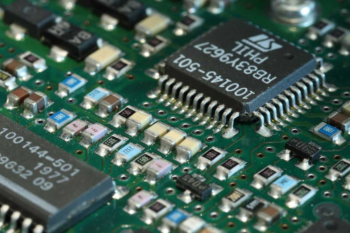
印刷电路板(或称 PCB)是大多数电子设备的基础,是通过 PCB 制造工艺实现的。印刷电路板的制作方法是在非导电基板上铺上薄铜片,然后蚀刻掉多余的铜片,形成所需的电路图案。
印刷电路板可以非常简单,只有几条铜线,也可以非常复杂,有几层相互连接的电路,有效地形成一个三维网。必须对制造过程进行严格控制,以确保印刷电路板成品符合所需的规格,不会出现缺失或断断续续的接触。
有几种方法可用于在印刷电路板上制作电路图案。选择哪种方法取决于所需图案的复杂程度。在印刷电路板上制作电路图案的主要常用方法是光刻法和蚀刻法。
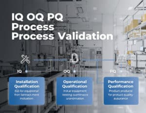
印刷电路板制造步骤

- Photolithography is a process of using light to create the desired circuit pattern on the PCB. This first step of the PCB manufacturing process begins with the application of a photosensitive resist onto the PCB surface, which is then selectively exposed to ultraviolet light through a mask that contains the desired circuit pattern. The exposure hardens the photosensitive material in the areas corresponding to the circuit design, while the unexposed areas remain soft and are subsequently removed during the development phase. This leaves a detailed pattern of the circuit on the board, allowing for the etching of the underlying material to create conductive paths. Photolithography allows for high precision and repeatability, making it possible to produce complex and densely packed circuits that are essential for modern electronic devices.
- 蚀刻 下一步是蚀刻掉裸露的铜,以形成所需的电路图案。根据铜的类型和所需的效果,可以使用多种不同的蚀刻化学药剂。一旦使用蚀刻溶液,它就会与裸露的铜发生反应,有效地腐蚀掉铜,而保护区域则不受影响。这种方法可以精确、高效地创建复杂的电路设计,是制造电子设备的重要步骤。随着时间的推移,先进的蚀刻技术和设备不断发展,提高了精度,减少了对环境的影响,进一步增强了印刷电路板生产的能力和可持续性。蚀刻完成后,剩余的光致抗蚀剂会被去除,在 PCB 上留下所需的电路图案。
- The next step is the application of solder mask, a protective layer that insulates the copper traces and prevents solder bridges during component placement. This is typically done through a process called solder mask application, where a liquid photoimageable film is applied and then cured using UV light.
- Next, the silkscreen process is employed to print component identifiers, logos, or other necessary markings on the board. Following this, the boards undergo a surface finish process, such as hot air solder leveling (HASL), immersion gold, or other methods, to prepare the copper pads for soldering by enhancing their solderability and protecting them from oxidation.
- Drilling is another critical step in PCB Manufacturing, where precise holes are created for component leads and vias, often using computer-controlled machines to ensure accuracy. Once drilling is complete, the boards may undergo plating to coat the drilled holes with copper, creating electrical connections between different layers.
- Finally, electrical testing ensures that the PCB functions as intended by checking for shorts, opens, and other defects. Each of these processes is vital to producing a reliable and high-quality printed circuit board ready for assembly.
以下两家印刷电路板制造工厂将对这些步骤进行更详细的介绍和说明,从订单接收到控制和包装,实现了以下令人印象深刻的关键绩效指标
- 从接受订单到发货的总交货时间:2 至 4 天
- 每天 5000 多份订单!
而这是针对单位订单,不一定是回头客,针对专业人士和非专业人士--这意味着需求中可能存在误差--以及整个过程中的一些设计和质量检查。受到启发!
At PCBway:
[embedyt] https://www.youtube.com/watch?v=24ehoo6RX8w[/embedyt]
And then how its main competitor does it, JLCPCB
[embedyt] https://www.youtube.com/watch?v=ljOoGyCso8s[/embedyt]
有关更多电子词汇、印刷电路板类型和元件基底面,请参阅《印刷电路板和电子参考资料详解》或维基百科。 印刷电路板制造 page.
相关阅读与方法
- 及时 (JIT) inventory management in PCB factories: analyze how JIT inventory methods can reduce holding costs and improve manufacturing efficiency.
- PCB design software: discuss various software tools and techniques for designing PCBs, including schematic capture and layout design.
- Material selection for PCBs: examine the different materials used in PCB manufacturing, such as FR-4, polyimide, and metal-core, and their impact on performance and cost.
- Thermal management in PCBs: investigate methods for managing heat in PCB design and manufacturing, including thermal vias, heat sinks, and thermal interface materials.
- PCB testing and inspection techniques: detail various testing and inspection methods, including automated optical inspection (AOI), in-circuit testing (ICT), and functional testing.
- Environmental considerations in PCB manufacturing: discuss the environmental impact of PCB manufacturing and methods for reducing waste and harmful emissions.
- Advanced PCB technologies: explore advancements in PCB technology, such as flexible PCBs, HDI (High-Density Interconnect) PCBs, and multi-layer PCBs.
有关电子印刷电路板制造的外部链接
(将鼠标悬停在链接上即可查看内容描述)
术语表
Automated Optical Inspection (AOI): 一种使用成像技术检测印刷电路板和其他电子组件中的缺陷的过程,通过根据预定标准分析视觉数据来确保质量控制并遵守规范。
Computed Tomography (CT): 一种医学成像技术,利用X射线和计算机处理技术创建人体横截面图像,从而能够详细地显示内部结构和组织。它通过从二维数据提供三维图像来增强诊断能力。
Cost Per Click (CPC): 一种数字广告定价模式,广告商每次广告被点击时都要支付费用。该模式衡量在线广告活动的成本效益,计算方法是将广告总支出除以实际点击次数。
Just In Time (JIT): 一种生产策略,旨在通过仅在制造过程中需要时接收货物来降低库存成本,从而最大限度地减少浪费并提高效率。
Key Performance Indicator (KPI): 一个可衡量的值,表明组织实现关键业务目标的效率,通常用于评估实现目标的成功程度。
Printed Circuit Board (PCB): 一种由绝缘材料制成的平板,用于支撑并通过导电通路连接电子元件,通常由铜片蚀刻而成。它作为电路组装的基础,并有助于元件之间的电气连接。


有趣的阅读!还有人认为印刷电路板制造技术的进步有可能颠覆传统方法吗?
每天数千份订单的周转时间如此之快!而且视频都是旧的!现在可能更多了!
通过视频,我们可以直观地了解到实现如此高精度和速度的复杂过程。
看到复杂的印刷电路板制造过程如何在短短 2 至 4 天内以如此高的效率和精度完成,真是令人着迷。来自 PCBway 和 JLCPCB 的视频提供了对该行业的深入了解,并突出了现代制造技术令人印象深刻的能力!
关于印刷电路板制造的文章很有意思。但是,采用人工智能自动化不是可以加快流程并显著提高效率吗?
读来有趣,但难道没有更环保的方法来处理多氯联苯废料吗?行业标准是什么?