Product Design, Manufacturing & Innovation Resources
家 » 互补金属氧化物半导体 (CMOS)

互补金属氧化物半导体 (CMOS)

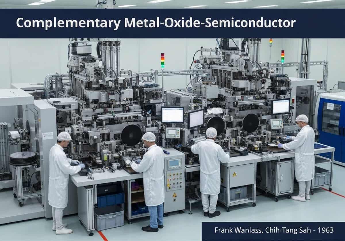
1963
  • Frank Wanlass
  • Chih-Tang Sah
Modern semiconductor fabrication facility focusing on CMOS technology and processes.

(图片仅供参考)

CMOS (Complementary Metal-Oxide-Semiconductor) is the dominant technology for constructing integrated circuits. It uses complementary pairs of p-type and n-type MOSFETs to build logic gates. Its primary advantage is very low static power consumption, as one transistor in the pair is always off during steady state, resulting in minimal current flow except during switching transitions.

A CMOS logic gate, such as an inverter, is constructed with both a PMOS (p-type) and an NMOS (n-type) transistor. The PMOS transistor is connected to the positive voltage supply (Vdd), and the NMOS transistor is connected to ground (GND). Their gates are tied together as the input, and their drains are tied together as the output. When the input is low (logic 0), the PMOS transistor turns on, and the NMOS turns off, pulling the output high to Vdd (logic 1). Conversely, when the input is high (logic 1), the PMOS turns off, and the NMOS turns on, pulling the output low to GND (logic 0).

In either stable state (output high or low), one of the transistors is off, creating a very high resistance path between the power supply and ground. This means that virtually no current flows, leading to extremely low static power dissipation. Power is primarily consumed only when the transistors are switching states. This characteristic made CMOS technology ideal for battery-powered devices and for creating highly dense integrated circuits where managing heat dissipation is a critical challenge. The scalability of CMOS, allowing for smaller and faster transistors with each generation, has been the engine behind Moore’s Law and the digital revolution.

UNESCO Nomenclature: 2205
– Electronics

类型

Physical Device

中断

Revolutionary

用法

广泛使用

前体

  • MOSFET的发明
  • p型和n型半导体掺杂的发展
  • 平面晶体管制造工艺
  • 集成电路的发明

应用程序

  • 微处理器
  • 微控制器
  • 静态随机存取存储器(sram)
  • 图像传感器
  • 最现代的数字逻辑电路

专利:

  • US3356858

潜在创新理念

  • 用于超低功耗物联网设备的亚阈值CMOS电路
  • 用于数码相机和智能手机的 CMOS 图像传感器
  • 绝缘体上硅 (SOI) CMOS,可提高性能和抗辐射能力
  • 3D CMOS集成,用于垂直堆叠多个电路层
  • 低温 cmos for quantum computer control interfaces
  • cmos-compatible mems (micro-electro-mechanical systems)
  • FinFET 和环绕栅极 (GAA) 晶体管是 CMOS 的演变
  • 用于医疗诊断的基于CMOS的生物传感器
Related to: cmos, mosfet, integrated circuit, low power, semiconductor, digital logic, microprocessor, transistor.

历史背景

互补金属氧化物半导体 (CMOS)

1960
1960-05-16
1962
1963
1964
1968
1970
1960
1960
1961
1962
1963
1965
1970
1970

(如果日期未知或不相关,例如“流体力学”,则提供其显著出现的近似估计)

第十年 周年纪念日

只有注册会员才能免费获取完整尺寸的图片和下载内容。

> 登录 <