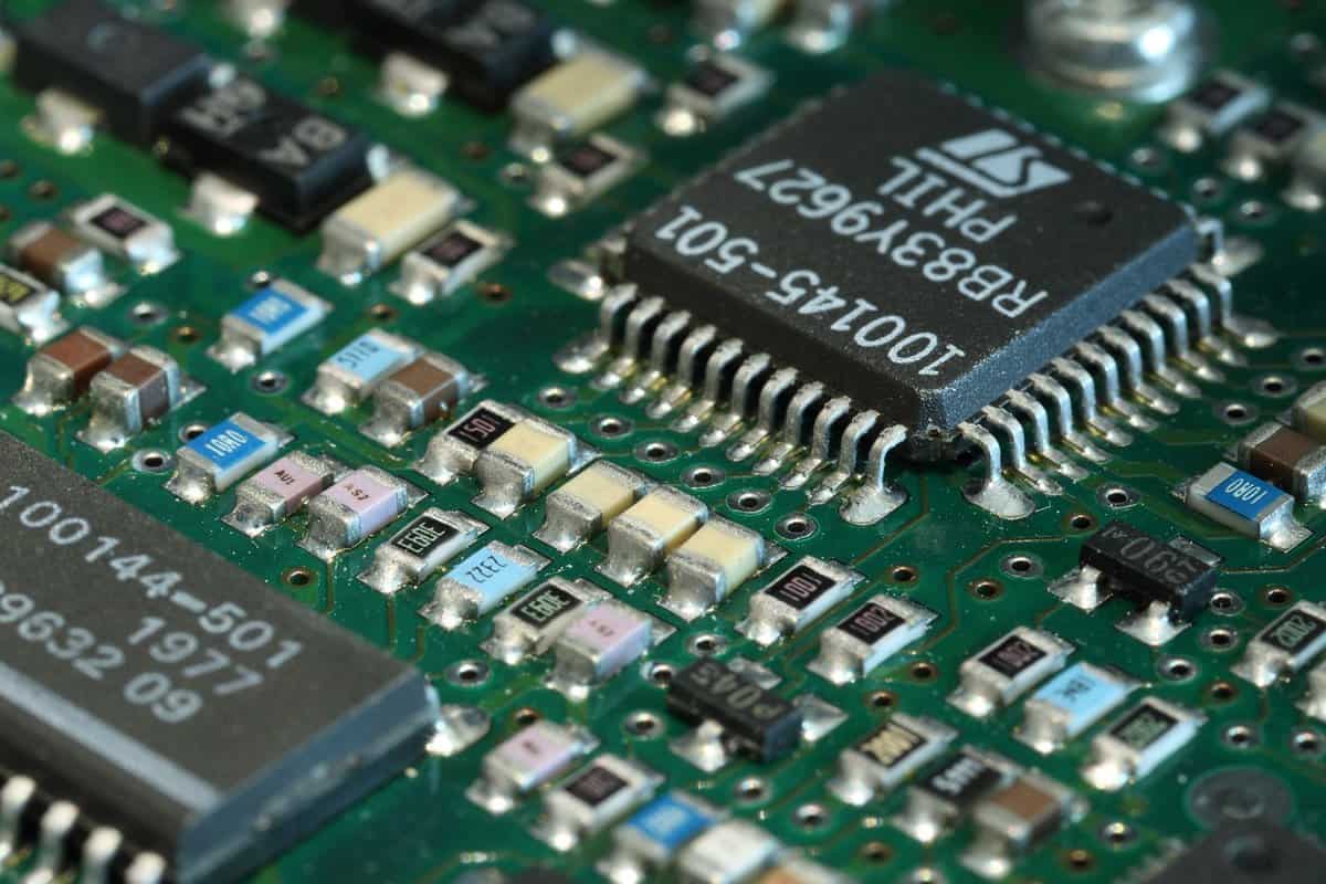
Printed circuit boards, or PCBs, are the foundation of most electronic devices and is achieved through the PCB manufacturing process. They are made by layering thin sheets of copper onto a non-conductive substrate, and then etching away the excess copper to create the desired circuit pattern.
PCBs can be very simple, with just a few copper traces, or extremely complex, with several layers of interconnecting circuitry, effectively forming a 3D mesh. The manufacturing process must be carefully controlled to ensure that the finished PCB meets the desired specifications without missing or intermittent contact.
There are several methods that can be used to create the circuit pattern on a PCB. The choice of method will depend on the complexity of the desired pattern. The key common methods, used also in the 2 videos below, for creating circuit patterns on PCBs are photolithography and etching.
PCB Manufacturing Steps

- Photolithography is a process of using light to create the desired circuit pattern on the PCB. This first step of the PCB manufacturing process begins with the application of a photosensitive resist onto the PCB surface, which is then selectively exposed to ultraviolet light through a mask that contains the desired circuit pattern. The exposure hardens the photosensitive material in the areas corresponding to the circuit design, while the unexposed areas remain soft and are subsequently removed during the development phase. This leaves a detailed pattern of the circuit on the board, allowing for the etching of the underlying material to create conductive paths. Photolithography allows for high precision and repeatability, making it possible to produce complex and densely packed circuits that are essential for modern electronic devices.
- Etching: this next step is to etch away the exposed copper to create the desired circuit pattern. There are many different etching chemicals that can be used, depending on the type of copper being used and the desired results. Once the etching solution is applied, it reacts with the exposed copper, efficiently eroding it away while the protected areas remain unaffected. This method allows for the precise and efficient creation of complex circuit designs, making it a vital step in the manufacturing of electronic devices. Advanced etching techniques and equipment have been developed over time to improve accuracy and reduce environmental impact, further enhancing the capabilities and sustainability of PCB production. Once the etching is complete, the remaining photoresist is removed, leaving behind the desired circuit pattern on the PCB.
- The next step is the application of solder mask, a protective layer that insulates the copper traces and prevents solder bridges during component placement. This is typically done through a process called solder mask application, where a liquid photoimageable film is applied and then cured using UV light.
- Next, the silkscreen process is employed to print component identifiers, logos, or other necessary markings on the board. Following this, the boards undergo a surface finish process, such as hot air solder leveling (HASL), immersion gold, or other methods, to prepare the copper pads for soldering by enhancing their solderability and protecting them from oxidation.
- Drilling is another critical step in PCB Manufacturing, where precise holes are created for component leads and vias, often using computer-controlled machines to ensure accuracy. Once drilling is complete, the boards may undergo plating to coat the drilled holes with copper, creating electrical connections between different layers.
- Finally, electrical testing ensures that the PCB functions as intended by checking for shorts, opens, and other defects. Each of these processes is vital to producing a reliable and high-quality printed circuit board ready for assembly.
These steps are shown in much more detail and explanations in the two PCB manufacturing factories hereafter, from order intake to control and packaging, achieving the impressive KPIs of
- total delivery time from order intake to shipping: 2 to 4 days
- 5000+ orders per day!
and this for unit orders, not necessarily returning customers, for pros and non-pros -meaning potential errors in the demand-, and some design and quality checks along the process. Be inspired!
At PCBway:
And then how its main competitor does it, JLCPCB
For further electronic vocabulary, PCB types, and components footprints, refer to the PCB and electronic reference detailed Post or Wikipedia PCB Manufacturing page.
Related Readings & Methodologies
- Just-In-Time (JIT) inventory management in PCB factories: analyze how JIT inventory methods can reduce holding costs and improve manufacturing efficiency.
- PCB design software: discuss various software tools and techniques for designing PCBs, including schematic capture and layout design.
- Material selection for PCBs: examine the different materials used in PCB manufacturing, such as FR-4, polyimide, and metal-core, and their impact on performance and cost.
- Thermal management in PCBs: investigate methods for managing heat in PCB design and manufacturing, including thermal vias, heat sinks, and thermal interface materials.
- PCB testing and inspection techniques: detail various testing and inspection methods, including automated optical inspection (AOI), in-circuit testing (ICT), and functional testing.
- Environmental considerations in PCB manufacturing: discuss the environmental impact of PCB manufacturing and methods for reducing waste and harmful emissions.
- Advanced PCB technologies: explore advancements in PCB technology, such as flexible PCBs, HDI (High-Density Interconnect) PCBs, and multi-layer PCBs.
External Links on Electronic PCB Manufacturing
International Standards
(hover the link to see our description of the content)
Glossary of Terms Used
Automated Optical Inspection (AOI): a process using imaging technology to detect defects in printed circuit boards and other electronic assemblies by analyzing visual data against predefined criteria, ensuring quality control and adherence to specifications.
Computed Tomography (CT): a medical imaging technique that uses X-rays and computer processing to create cross-sectional images of the body, allowing for detailed visualization of internal structures and tissues. It enhances diagnostic capabilities by providing three-dimensional representations from two-dimensional data.
Cost Per Click (CPC): a digital advertising pricing model where advertisers pay a fee each time their ad is clicked. It measures the cost-effectiveness of online campaigns, calculated by dividing total ad spend by the number of clicks received.
Just In Time (JIT): a production strategy that aims to reduce inventory costs by receiving goods only as they are needed in the manufacturing process, thereby minimizing waste and increasing efficiency.
Key Performance Indicator (KPI): a measurable value that demonstrates how effectively an organization is achieving key business objectives, often used to evaluate success at reaching targets.
Printed Circuit Board (PCB): a flat board made of insulating material that supports and connects electronic components through conductive pathways, typically etched from copper sheets. It serves as a foundation for circuit assembly and facilitates electrical connections between components.