Home » Complementary Metal-Oxide-Semiconductor (CMOS)

Complementary Metal-Oxide-Semiconductor (CMOS)

1963
  • Frank Wanlass
  • Chih-Tang Sah

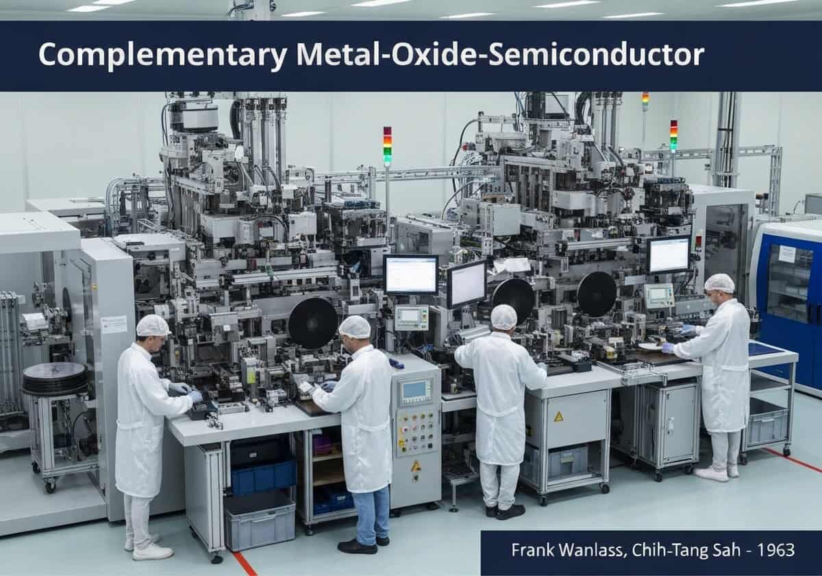
CMOS (Complementary Metal-Oxide-Semiconductor) is the dominant technology for constructing integrated circuits. It uses complementary pairs of p-type and n-type MOSFETs to build logic gates. Its primary advantage is very low static power consumption, as one transistor in the pair is always off during steady state, resulting in minimal current flow except during switching transitions.

A CMOS logic gate, such as an inverter, is constructed with both a PMOS (p-type) and an NMOS (n-type) transistor. The PMOS transistor is connected to the positive voltage supply (Vdd), and the NMOS transistor is connected to ground (GND). Their gates are tied together as the input, and their drains are tied together as the output. When the input is low (logic 0), the PMOS transistor turns on, and the NMOS turns off, pulling the output high to Vdd (logic 1). Conversely, when the input is high (logic 1), the PMOS turns off, and the NMOS turns on, pulling the output low to GND (logic 0).

In either stable state (output high or low), one of the transistors is off, creating a very high resistance path between the power supply and ground. This means that virtually no current flows, leading to extremely low static power dissipation. Power is primarily consumed only when the transistors are switching states. This characteristic made CMOS technology ideal for battery-powered devices and for creating highly dense integrated circuits where managing heat dissipation is a critical challenge. The scalability of CMOS, allowing for smaller and faster transistors with each generation, has been the engine behind Moore’s Law and the digital revolution.

UNESCO Nomenclature: 2205
– Electronics

Type

Physical Device

Disruption

Revolutionary

Usage

Widespread Use

Precursors

  • Invention of the MOSFET
  • Development of p-type and n-type semiconductor doping
  • Planar process for manufacturing transistors
  • Invention of the integrated circuit

Applications

  • microprocessors
  • microcontrollers
  • static ram (sram)
  • image sensors
  • most modern digital logic circuits

Patents:

  • US3356858

Potential Innovations Ideas

Professionals (100% free) Membership Required

You must be a Professionals (100% free) member to access this content.

Join Now

Already a member? Log in here
Related to: cmos, mosfet, integrated circuit, low power, semiconductor, digital logic, microprocessor, transistor

Leave a Reply

Your email address will not be published. Required fields are marked *

AVAILABLE FOR NEW CHALLENGES
Mechanical Engineer, Project or R&D Manager
Effective product development

Available for a new challenge on short notice.
Contact me on LinkedIn
Plastic metal electronics integration, Design-to-cost, GMP, Ergonomics, Medium to high-volume devices & consumables, Regulated industries, CE & FDA, CAD, Solidworks, Lean Sigma Black Belt, medical ISO 13485

We are looking for a new sponsor


Your company or institution is into technique, science or research ?
> send us a message <

Receive all new articles
Free, no spam, email not distributed nor resold

or you can get your full membership -for free- to access all restricted content >here<

Related Invention, Innovation & Technical Principles

Scroll to Top

You May Also Like