Top-Down Nanomaterial Synthesis
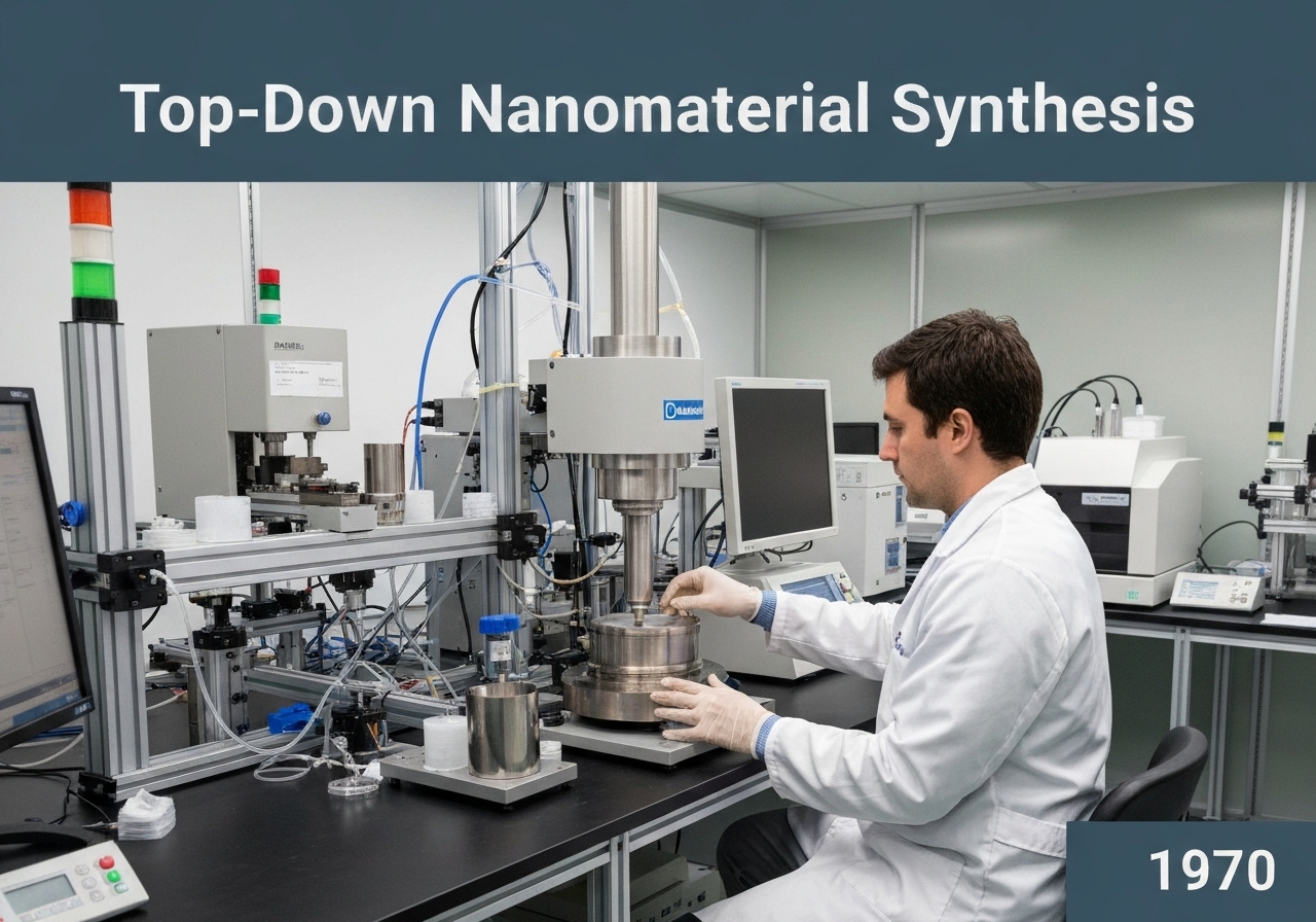
Top-down synthesis involves creating nanomaterials by starting with a larger, bulk material and breaking it down or patterning it to the nanoscale. Key techniques include mechanical methods like ball milling and lithographic methods like photolithography, electron-beam lithography, and nanoimprint lithography. These methods are often used for creating structured surfaces and integrated circuits, but can suffer from surface imperfections.
Top-down approaches are conceptually straightforward: they are an extension of traditional microfabrication techniques to smaller dimensions. The most prominent example is lithography, the cornerstone of the semiconductor industry. In photolithography, a light-sensitive polymer (photoresist) is coated onto a substrate. A mask is used to selectively expose the resist to UV light, causing a chemical change that allows for the selective removal of either the exposed or unexposed regions. The underlying material can then be etched or deposited upon, transferring the pattern from the mask to the substrate. To achieve nanoscale features, shorter wavelength light sources (e.g., extreme ultraviolet, EUV) or alternative patterning sources like electron beams (e-beam lithography) are used. E-beam lithography offers very high resolution but is a slow, serial process, making it unsuitable for mass production but excellent for prototyping and mask making.
Another major class of top-down methods is mechanical attrition. High-energy ball milling, for instance, places a bulk material in a container with hard grinding media (balls). The container is rotated at high speed, causing the balls to collide with and fracture the material, progressively reducing its particle size down to the nanometer scale. This method is simple and scalable for producing large quantities of nanopowders but offers poor control over particle shape and size distribution, and can introduce impurities from the milling media.
The primary advantage of top-down methods, particularly lithography, is the ability to create precisely ordered and complex structures over large areas, which is essential for integrated circuits. However, a significant drawback is the introduction of crystallographic damage and surface defects during the etching or milling process, which can negatively impact the material’s properties.
UNESCO Nomenclature: 2211
– Solid state physics
Precursors
- invention of the printing press and early lithographic printing
- development of photography and photosensitive chemicals
- the invention of the transistor and the subsequent drive for miniaturization in electronics
- advances in vacuum technology and plasma physics for etching processes
Applications
- manufacturing of computer microprocessors and memory chips
- fabrication of microelectromechanical systems (mems)
- creation of patterned surfaces for biomedical applications
- production of nanopowders for ceramics and composites
- fabrication of molds for nanoimprint lithography
Potential Innovations Ideas
Due to scrapping bot traffic, currently more than 40k per day, this content is reserved to community members.
> Login < or > Register < (100% free) to access this, so as all other restricted content and tools.
Related to: top-down synthesis, lithography, photolithography, e-beam lithography, ball milling, microfabrication, semiconductor, etching, nanopatterning, mems.