Product Design, Manufacturing & Innovation Resources

Neueste Veröffentlichungen & Patente für fortschrittliche Halbleitergehäuse

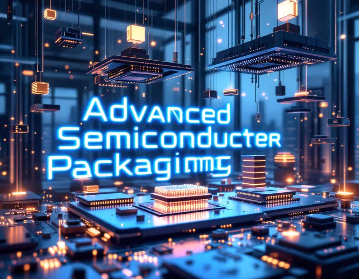
Advanced Semiconductor Packaging

Tipp: Zusätzlich zu der unten stehenden Auswahl können Sie unsere 2 gesamten Datenbanken durchsuchen und filtern:

> Kostenloses Tool zur Suche nach Veröffentlichungen < nach Autor, Thema, Stichwörtern, Datum oder Zeitschrift.

> Kostenloses Tool zur Suche nach Patenten < für Patente in englischer Sprache vom Europäischen Patentamt.

Advanced semiconductor packaging
Advanced semiconductor packaging innovations enhance system performance through chiplet integration and 3d stacking, while addressing manufacturing and thermal challenges.

Advanced semiconductor packaging has become a primary lever for system performance as transistor scaling slows. Instead of one large monolithic die, designers assemble chiplets, memory stacks and photonic elements on silicon interposers, organic substrates or glass cores. 2.5D integration places dies side by side on a shared interposer. 3D stacking uses through-silicon vias and hybrid bonding to reach interconnect pitches below 10 micrometers. High bandwidth memory is the most visible commercial example.

Manufacturing and thermal constraints dominate. Warpage, die shift, voids in underfill and thermomechanical stress from mismatched coefficients of thermal expansion all degrade yield. Heat extraction from stacked logic remains an open problem, as does known-good-die testing before assembly. Co-packaged optics adds alignment and reliability questions. The publications and patents indexed below address bonding processes, interposer and substrate design, test access, thermal solutions and die-to-die interconnect standards.

1
Behandelte Themen: Advanced Semiconductor Packaging, chiplets, heterogeneous integration, 2.5D integration, 3D stacking, through-silicon vias, hybrid bonding, silicon interposers, glass substrates, fan-out wafer-level packaging, high bandwidth memory, co-packaged optics, underfill, warpage, thermal interface materials, JESD235, JESD22-A104, IEEE 1838 and UCIe..

Historischer Kontext

1965
1970
1970
1974-11-15
1980
1980
1980
1964
1968
1970
1970
1975
1980
1980
1980

(wenn das Datum unbekannt oder nicht relevant ist, z. B. „Strömungsmechanik“, wird eine gerundete Schätzung seines bemerkenswerten Auftretens bereitgestellt)

10. Jahr Jubiläum

Bilder in voller Größe und Downloads sind ausschließlich für registrierte Mitglieder kostenlos verfügbar.

> Login <