
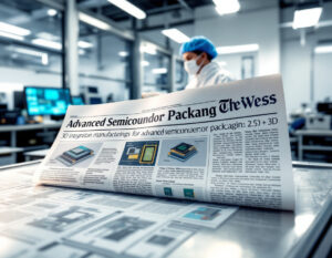
Advanced semiconductor packaging has become a primary lever for system performance as transistor scaling slows. Instead of one large monolithic die, designers assemble chiplets, memory stacks and photonic elements on silicon interposers, organic substrates or glass cores. 2.5D integration places dies side by side on a shared interposer. 3D stacking uses through-silicon vias and hybrid bonding to reach interconnect pitches below 10 micrometers. High bandwidth memory is the most visible commercial example.
Manufacturing and thermal constraints dominate. Warpage, die shift, voids in underfill and thermomechanical stress from mismatched coefficients of thermal expansion all degrade yield. Heat extraction from stacked logic remains an open problem, as does known-good-die testing before assembly. Co-packaged optics adds alignment and reliability questions. The publications and patents indexed below address bonding processes, interposer and substrate design, test access, thermal solutions and die-to-die interconnect standards.
1