
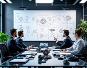
A complete overview of modern electronic board manufacturing.
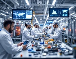
Shows two assembly and brazing technics, depending on the components used:
- SMT (Surface Mound Technology) for smaller components
- wave soldering, for bigger components using the so-called through-hole technology where wire leads pass through the PCB.
Automatic visual inspection, so as electrical control is then performed on 100% of production. To notice also the interesting lean benches for manual operations and how the instructions are given by video to the operator.

Be sure to check the two other PCB Factory Tours done in China


Interesting read but arent we overlooking the e-waste issue created by such circuit board assembly processes? Thoughts?
Indeed, but isnt progress always trailed by its own set of problems?
Quantum computing isnt replacing circuit boards anytime soon. They coexist, not compete. Research before commenting!
Circuit board assembly should be taught in high school
Why not use AI for circuit board assembly? Surely, itd minimize errors and increase efficiency. Just food for thought, guys.
AI isnt flawless! Relying on it completely could result in unexpected failures. Humans are irreplaceable.