Product Design, Manufacturing & Innovation Resources
家 » カーボンナノチューブ電界効果トランジスタ(CNTFET)

カーボンナノチューブ電界効果トランジスタ(CNTFET)

1998
  • Sumio Iijima
  • Cees Dekker
  • Phaedon Avouris
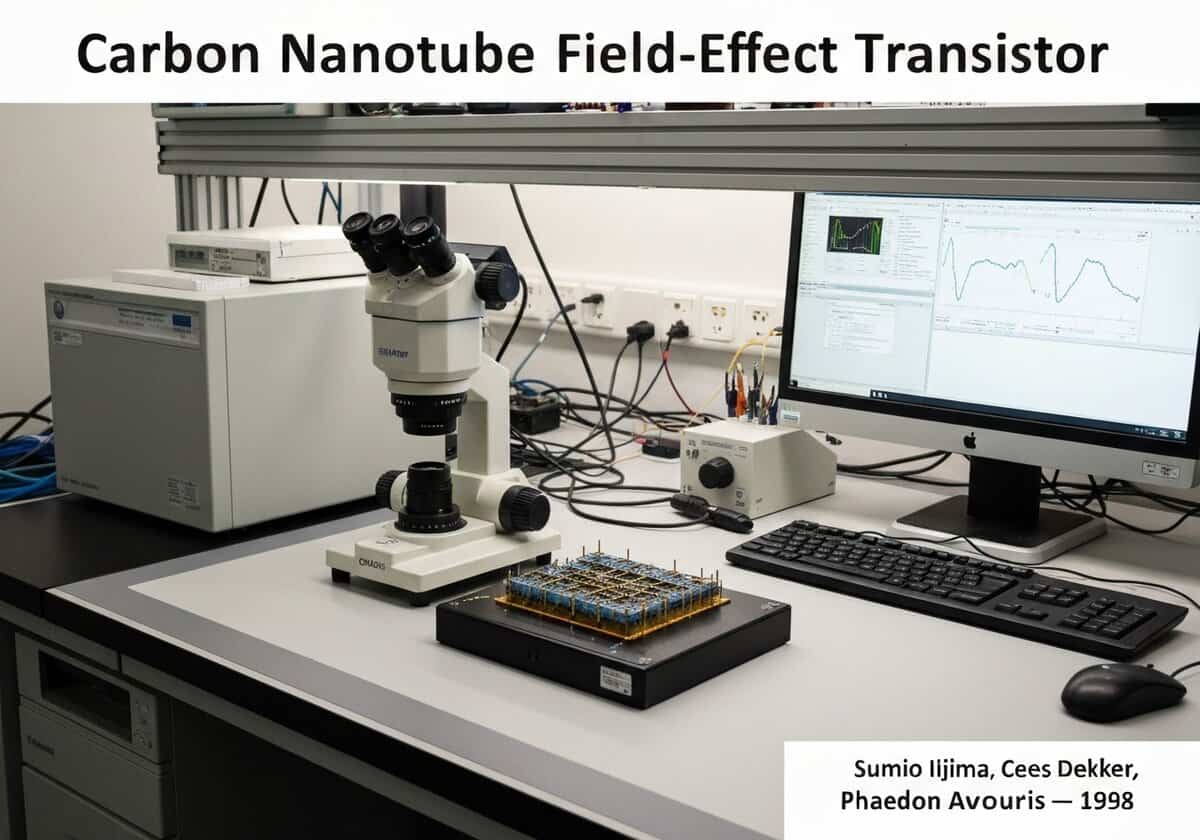
Carbon Nanotube Field-Effect Transistor in a laboratory setting, materials science application.

(画像はイメージです)

あ Carbon Nanotube 電界効果 トランジスタ (CNTFET) utilizes a single carbon nanotube (CNT) or an array of CNTs as the channel material instead of bulk silicon. Depending on its chirality (the arrangement of its graphene lattice), a CNT can be either metallic or semiconducting, making it a versatile building block for nanoelectronic devices with superior performance potential.


A CNTFET operates on the same principle as a conventional MOSFET. It has a source, a drain, and a gate terminal. The key difference is the channel, which is formed by one or more carbon nanotubes. When a voltage is applied to the gate, it creates an electric field that modulates the conductivity of the semiconducting CNT, turning the flow of current between the source and drain ‘on’ or ‘off’. The exceptional properties of CNTs make them highly attractive for this application. They exhibit extremely high carrier mobility, meaning electrons can travel through them with very little 散乱これは、スイッチング速度の向上と電流容量の増加につながります。また、一次元構造によりゲートによる優れた静電制御が可能となり、小型化されたシリコントランジスタによく見られる短チャネル効果を低減します。

しかしながら、CNTFETの普及には大きな課題が立ちはだかっている。その大きな障害の一つがCNTの合成である。一般的な合成方法では、金属型ナノチューブと半導体型ナノチューブが混在して生成される。金属型ナノチューブは短絡として働き、トランジスタの完全なオフオフを妨げ、高い電力リークを引き起こす。これらのナノチューブを100%の純度で大規模に分離することは困難かつ高コストである。もう一つの課題は、CNTをウェハ上に正確な位置合わせと密度で配置することである。さらに、ナノチューブの両端に低抵抗の電気接点を形成することも容易ではなく、デバイス全体の性能を制限する要因となる。

こうした課題にもかかわらず、研究は大きな進歩を遂げている。金属CNTを選択的に除去したり、半導体CNTに変換したりする技術が開発されてきた。16ビットマイクロプロセッサを含む複雑な回路がCNTFETを用いて構築され、この技術の実現可能性が実証されている。また、CNTの独自の特性により、標的分子が付着するとCNTの導電率が劇的に変化する高感度バイオセンサーなどの新しい用途や、本来の機械的強度と柔軟性からフレキシブルエレクトロニクスにも最適である。

UNESCO Nomenclature: 3313
材料科学

タイプ

物理デバイス

混乱

実質的な

使用法

新興技術

前駆物質

  • invention of the field-effect トランジスタ (FET)
  • フラーレンの発見
  • カーボンナノチューブの発見と合成
  • 半導体製造技術(リソグラフィー、蒸着)の開発

アプリケーション

  • 高周波エレクトロニクス
  • 化学センサーおよびバイオセンサー
  • 柔軟で透明な電子機器
  • 将来の論理回路におけるシリコンの代替品となる可能性

特許:

  • US6835601B2
  • US7015501B2

潜在的なイノベーションのアイデア

  • self-powered sensors that harvest energy from ambient vibrations using piezoelectric CNTs
  • radiation-hardened electronics for space applications
  • terahertz-frequency communication devices
  • implantable neural interfaces with high biocompatibility
  • transparent transistors for heads-up displays integrated into eyeglasses
  • ultra-efficient thermoelectric generators using CNT arrays
  • spin-based logic devices using magnetic contacts on CNTs
  • artificial 光合成 systems using CNTs as charge separation and transport channels
Related to: CNTFET, carbon nanotube, field-effect transistor, carrier mobility, chirality, nanoelectronics, post-silicon technology, flexible electronics.

歴史的背景

カーボンナノチューブ電界効果トランジスタ(CNTFET)

1992
1993-07-22
1996
1998
1999
2000
2000
1992
1993
1994
1997
1998
1999-05-01
2000
2000

(日付が不明または関連性がない場合、例えば「流体力学」などでは、その注目すべき出現時期の概算値が提示されます。)

10年目 周年

フルサイズの画像とダウンロードは、登録会員のみが100%無料で利用できます。