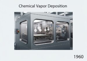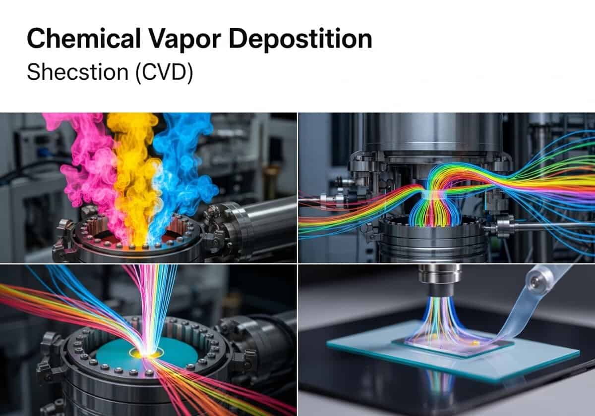
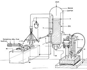
La deposizione chimica da vapore (CVD) è una delle principali tecniche di film tecnica di fabbricazione che prevede reazioni chimiche di precursori in fase vapore su substrati riscaldati per produrre rivestimenti conformali di elevata purezza con un controllo preciso dello spessore e della composizione. Questo settore integra le interazioni tra la chimica dei precursori, la dinamica dei flussi di gas, le reazioni superficiali e la gestione termica all'interno di reattori specializzati. Le applicazioni spaziano dalla produzione di dispositivi a semiconduttore, ai rivestimenti protettivi, alla sintesi di materiali avanzati. La seguente raccolta presenta le più recenti pubblicazioni e brevetti sottoposti a peer-review, che riflettono i progressi nella progettazione di reattori, nello sviluppo di precursori, nell'ottimizzazione dei processi e nelle nuove modalità di CVD, come la CVD al plasma e quella metallo-organica.
Questa è la nostra ultima selezione di pubblicazioni e brevetti in inglese sulla deposizione chimica da vapore (CVD), tra numerose riviste scientifiche online, classificate e focalizzate su CVD, deposizione chimica da vapore, deposizione di film sottili, gas precursore, riscaldamento del substrato, velocità di deposizione, uniformità del film, dinamica del flusso di gas, reazioni superficiali, nucleazione, meccanismo di crescita del film, CVD termica, CVD potenziata al plasma, CVD metallo-organica, deposizione di strati atomici, ALD, temperatura di deposizione, gas vettore, controllo dello spessore del film, conformità, pressione di deposizione, precursori chimici, morfologia del film, cinetica di deposizione, reazioni in fase gassosa, diffusione superficiale, reattore CVD e selettività di deposizione.
Processing method and processing device
Patent published on the 2026-07-02 in WO under Ref WO2026140956 by TOKYO ELECTRON LTD [JP] (Takezawa Yoshihiro [jp], Miyahara Tatsuya [jp], Hayashi Ryunosuke [jp])
Abstract: A processing method according to one embodiment of the present disclosure comprises: preparing a substrate that has a catalyst-metal-containing polycrystalline silicon film on the surface thereof; forming a gettering layer formed of amorphous silicon on the polycrystalline silicon film through chemical vapor deposition using an organoaminosilane gas; and annealing the substrate to diffuse the catalyst metal contained in the polycrystalline silicon film into the gettering layer.[...]
Our summary: The processing method involves preparing a substrate with a catalyst-metal-containing polycrystalline silicon film. A gettering layer of amorphous silicon is formed on this film using chemical vapor deposition. The substrate is then annealed to diffuse the catalyst metal into the gettering layer.
catalyst, polycrystalline silicon, chemical vapor deposition, annealing
Patent
Film and method for producing same
Patent published on the 2026-07-02 in WO under Ref WO2026141357 by TOAGOSEI CO LTD [JP] (Sasagawa Keita [jp], Yasuhara Shigeo [jp])
Abstract: Provided is a method for producing a film containing Sn and Ge, which includes: an Sn film formation step for forming an Sn-containing film using a tin compound as a starting material gas; and a Ge film formation step for forming a Ge-containing film using a germanium compound as a starting material gas. The film formation is performed by a chemical vapor deposition method or an atomic layer deposition method by supplying the starting material gas into a chamber in which an object to be processe[...]
Our summary: The method produces a film containing tin (Sn) and germanium (Ge). It involves forming an Sn-containing film using a tin compound and a Ge-containing film using a germanium compound. The film formation occurs through chemical vapor deposition or atomic layer deposition techniques.
Sn film, Ge film, chemical vapor deposition, atomic layer deposition
Patent
Film and method for producing same
Patent published on the 2026-07-02 in WO under Ref WO2026141475 by TOAGOSEI CO LTD [JP] (Sasagawa Keita [jp], Yasuhara Shigeo [jp])
Abstract: Provided is a method for producing a film containing Sn and Si, which includes: an Sn film formation step for forming an Sn-containing film using a tin compound as a starting material gas; and an Si film formation step for forming an Si-containing film using a silicon compound as a starting material gas. The film formation is performed by a chemical vapor deposition method or an atomic layer deposition method by supplying the starting material gas into a chamber in which an object to be processe[...]
Our summary: The method involves forming an Sn-containing film using a tin compound and an Si-containing film using a silicon compound. Both film formations are executed through chemical vapor deposition or atomic layer deposition. The process takes place in a chamber with a film formation surface on the object being processed.
Sn film, Si film, chemical vapor deposition, atomic layer deposition
Patent
Method and apparatus for reducing wastewater to concentrated wastewater
Patent published on the 2026-07-02 in WO under Ref WO2026141657 by NANOMIST TECH CO LTD [JP] (Matsuura Kazuo [jp])
Abstract: The present invention produces concentrated wastewater by efficiently separating excess water from a large amount of wastewater, and furthermore, efficiently separates effluent by membrane separation from the excess water separated from the wastewater, thereby reducing wastewater for disposal to concentrated wastewater. This method for separating excess water 2 from wastewater 1 and reducing the result to concentrated wastewater 3 comprises: a first separation step for separating the excess wate[...]
Our summary: The invention reduces wastewater by separating excess water from it. It employs ultrasonic atomization to create mist for efficient separation. A membrane separation step further isolates impurities from the excess water.
wastewater treatment, membrane separation, ultrasonic atomization, effluent recovery
Patent
Glass member, glass member manufacturing system, and glass member manufacturing method
Patent published on the 2026-07-02 in WO under Ref WO2026140211 by KOTO ELECTRIC CO LTD [JP] (Inoue Kotoku [jp], Takayama Masatoshi [jp])
Abstract: This glass member comprises a glass substrate, and a copper-containing conductive layer formed on the glass substrate. In the conductive layer, the number of blisters having a longest diameter of 5 μm or more is 5 blisters/cm2 or less. This glass member manufacturing system is provided with an electroless plating apparatus that forms a first metal film containing copper on a glass substrate, by electroless plating at a deposition rate of 1.3 μm/hour or less.[...]
Our summary: This content describes a glass member with a copper-containing conductive layer and specific blister limitations. It details a manufacturing system that utilizes electroless plating to create a metal film on the glass substrate. The plating process is characterized by a controlled deposition rate of 1.3 μm/hour or less.
glass member, conductive layer, electroless plating, manufacturing system
Patent
Method for manufacturing semiconductor thin film and method for manufacturing semiconductor device
Patent published on the 2026-07-02 in WO under Ref WO2026141249 by NATIONAL UNIVERSITY CORPORATION KYOTO INST OF TECHNOLOGY [JP] (Hosaka Shoma [jp], Nishinaka Hiroyuki [jp], Kaneko Masahiro [jp])
Abstract: This method for manufacturing a semiconductor thin film comprises a step for preparing a substrate formed of Ga2O3 crystal, and a step for forming a semiconductor thin film formed of (InxAl1-x)2O3 crystal on the substrate by a mist CVD method. Then, in the step for forming the semiconductor thin film, a raw material solution obtained by dissolving a precursor raw material containing indium acetylacetonate (In(C5H7O2)3) and aluminum acetylacetonate (Al(C5H7O2)3) in methanol is atomized and suppli[...]
Our summary: This method involves preparing a Ga2O3 substrate and forming a semiconductor thin film of (InxAl1-x)2O3 using a mist CVD technique. A raw material solution containing indium and aluminum acetylacetonate is atomized and applied to the substrate. The process enables the manufacturing of advanced semiconductor devices.
semiconductor, thin film, mist CVD, Ga2O3
Patent
dispersion cohesion, surface energy, and charging
Published on 2026-06-24 by Johannes Fiedler and Justas Zalieckas @IOP SCIENCE
Abstract: The formation of molecular clusters in low-temperature plasmas is governed by an intricate interplay of dispersion interactions, electrostatic charging, and surface energetics. While chemical growth pathways have been extensively studied, the role of non-chemical interactions in determining characteristic cluster sizes remains poorly understood. In this work, we develop a unified free-energy framework for molecular clusters embedded in weakly ionised Ar/H plasmas. The approach combines first-pri[...]
Our summary: The study develops a free-energy framework for molecular clusters in low-temperature plasmas. It combines first-principles calculations with a dielectric description of plasma response. Results indicate that plasma conditions control nucleation scales rather than free-energy minimization.
dispersion interactions, electrostatic charging, surface energetics, molecular clusters
Publication
Heralded linear optical generation of Dicke states
Published on 2026-04-30 by Minhyeok Kang, Jaehee Kim, William J Munro, Seungbeom Chin and Joonsuk Huh @IOP SCIENCE
Abstract: Entanglement is a fundamental feature of quantum mechanics and a key resource for quantum information processing. Among multipartite entangled states, Dicke states are distinguished by their permutation symmetry, which provides robustness against particle loss and enables applications for quantum communication and computation. Although Dicke states have been realized in various platforms, most optical implementations rely on postselection, which destroys the state upon detection and prevents its[...]
Our summary: This work presents a linear-optical heralded scheme for generating arbitrary Dicke states using photons. The approach leverages the permutation symmetry of Dicke states to simplify the generation process. This method offers a resource-efficient pathway for practical applications in quantum technologies.
Dicke states, quantum entanglement, linear optics, heralded generation
Publication