Product Design, Manufacturing & Innovation Resources
Home » Chemical Vapor Deposition (CVD)

Chemical Vapor Deposition (CVD)

1960
CVD chamber for semiconductor fabrication with substrate and chemical precursors.

(generated image for illustration only)

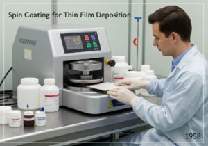
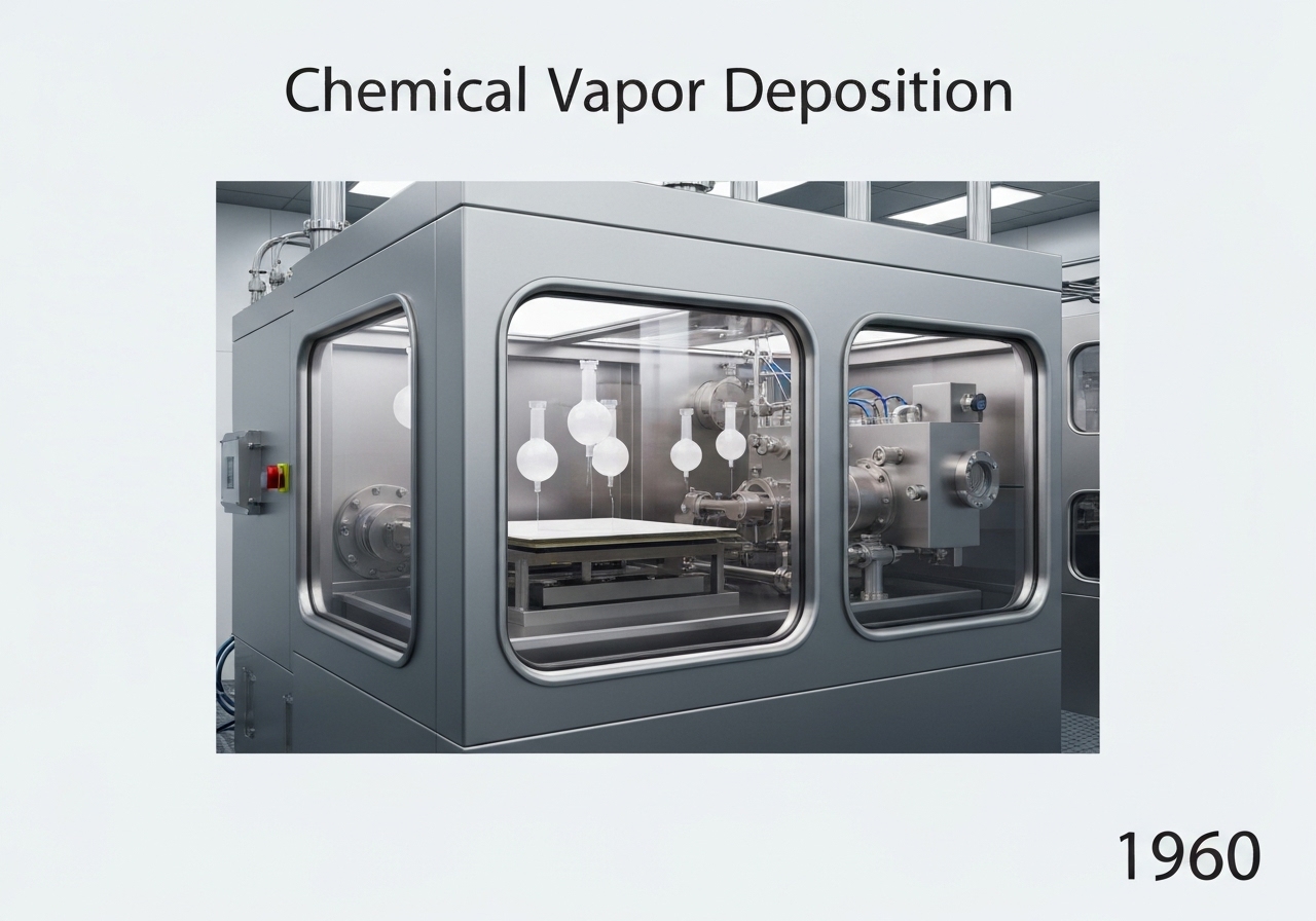
Chemical Vapor Deposition (CVD) is a coating process where a substrate is exposed to one or more volatile chemical precursors. These precursors react or decompose on the substrate’s surface in a reaction chamber, producing a high-purity, high-performance solid thin film or coating. Temperature and pressure are critical process parameters that control the deposition rate and film quality.

CVD is a highly versatile process capable of producing a wide variety of materials, including metals, ceramics, and polymers. The process begins with the introduction of gaseous precursor molecules into a vacuum chamber containing the heated substrate. The high temperature of the substrate provides the energy needed to break the chemical bonds in the precursor molecules, a process known as pyrolysis. The resulting reactive species then adsorb onto the substrate surface, diffuse, and react to form a stable solid film. Byproducts of the reaction are then desorbed and pumped out of the chamber. There are numerous variations of CVD, each tailored for specific applications. For example, Metalorganic CVD (MOCVD) uses metalorganic precursors and is crucial for manufacturing compound semiconductor devices like LEDs. Plasma-Enhanced CVD (PECVD) uses a plasma to energize the precursor gases, allowing deposition at lower temperatures, which is essential for substrates that cannot withstand high heat. Atomic Layer Deposition (ALD), a subtype of CVD, involves sequential, self-limiting surface reactions, enabling the deposition of films with atomic-level thickness control. The quality, stoichiometry, and morphology of the deposited film are precisely controlled by adjusting parameters like substrate temperature, chamber pressure, gas flow rates, and precursor chemistry.

UNESCO Nomenclature: 3322
– Technology of materials

Type

Chemical Process

Disruption

Foundational

Usage

Widespread Use

Precursors

  • understanding of gas-phase chemical kinetics
  • development of vacuum technology
  • synthesis of volatile chemical compounds (precursors)
  • advances in high-temperature furnace technology
  • theories of nucleation and film growth

Applications

  • semiconductor device fabrication (e.g., silicon dioxide, silicon nitride, polysilicon layers)
  • production of hard coatings for cutting tools (e.g., titanium nitride)
  • manufacturing of optical fibers
  • creation of synthetic diamonds
  • corrosion and high-temperature resistant coatings for aerospace components

Patents:

NA

Potential Innovations Ideas

Due to scrapping bot traffic, currently more than 40k per day, this content is reserved to community members.
> Login < or > Register < (100% free) to access this, so as all other restricted content and tools.

Related to: cvd, chemical vapor deposition, thin film, semiconductor, precursor, deposition, coating, plasma, mocvd, surface engineering.

Historical Context

Chemical Vapor Deposition (CVD)

1960
1960
1960
1960
1960
1960
1960
1958
1960
1960
1960
1960
1960
1960
1960

(if date is unknown or not relevant, e.g. "fluid mechanics", a rounded estimation of its notable emergence is provided)

Related Invention, Innovation & Technical Principles

Full size images and downloads are only available, 100% free, for registered members.

> Login <