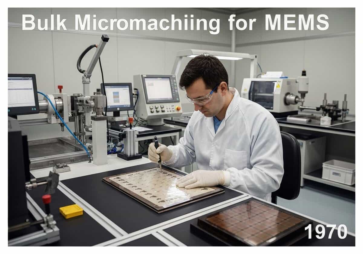
Bulk Micromachining for MEMS
Bulk micromachining is a subtractive fabrication process that creates MEMS structures by selectively etching into a substrate, typically a silicon wafer. It uses wet or dry etching techniques to sculpt the bulk material. Anisotropic etchants like potassium hydroxide (KOH) are common, as they etch different crystal planes of silicon at different rates, enabling the creation of precise V-grooves and cavities.
Bulk micromachining is one of the oldest and most established methods for creating MEMS. As a subtractive process, it involves sculpting the device’s features directly from the bulk of a substrate, usually a single-crystal silicon wafer. The technique relies heavily on etching, which can be broadly categorized as wet (chemical) or dry (plasma-based).
Wet etching is the more traditional approach. It can be isotropic, etching at the same rate in all directions, which results in rounded, undercut features. More commonly for MEMS, anisotropic wet etching is used. This method exploits the fact that the etch rate in single-crystal silicon depends on the crystallographic orientation. Etchants like potassium hydroxide (KOH), tetramethylammonium hydroxide (TMAH), and ethylenediamine pyrocatechol (EDP) etch the (100) and (110) crystal planes much faster than the (111) planes. By aligning the mask pattern with the crystal axes on a (100)-oriented wafer, this property can be used to create precisely defined structures with angled sidewalls, such as V-grooves for fiber optics or pyramidal pits. The (111) planes act as natural etch-stops, allowing for excellent control over the final geometry. Diaphragms for pressure sensors are a classic application, formed by etching from the backside of a wafer until an etch-stop layer (like a heavily doped boron layer or an electrochemical stop at a p-n junction) is reached.
Dry etching, particularly Deep Reactive-Ion Etching (DRIE), has become a dominant bulk micromachining technique. DRIE allows for the creation of very deep, high-aspect-ratio structures with nearly vertical sidewalls, something not possible with wet etching. The most common method is the ‘Bosch process,’ which alternates between an etching step (using a plasma like SF6) and a passivation step (using a polymerizing gas like C4F8). The passivation layer protects the sidewalls from being etched, forcing the etch to proceed primarily in the vertical direction. This cycle is repeated hundreds or thousands of times to achieve depths of hundreds of microns. DRIE is essential for manufacturing modern high-performance inertial sensors, microfluidic devices, and through-silicon vias (TSVs) for 3D chip stacking.
UNESCO Nomenclature: 3313
– Industrial Engineering
Precursors
- crystal orientation knowledge in silicon wafers
- development of chemical etchants for silicon
- photolithography for pattern definition
- masking materials resistant to etchants (e.g., silicon nitride)
Applications
- pressure sensor diaphragms
- inkjet printer nozzles
- microfluidic channels
- atomic force microscope (AFM) cantilevers
- v-grooves for optical fiber alignment
Potential Innovations Ideas
Due to scrapping bot traffic, currently more than 40k per day, this content is reserved to community members.
> Login < or > Register < (100% free) to access this, so as all other restricted content and tools.
Related to: bulk micromachining, MEMS, etching, silicon, anisotropic etching, KOH, DRIE, deep reactive-ion etching, subtractive process, microfabrication.