Product Design, Manufacturing & Innovation Resources
家 » 相補型金属酸化膜半導体(CMOS)

相補型金属酸化膜半導体(CMOS)

1963
  • Frank Wanlass
  • Chih-Tang Sah
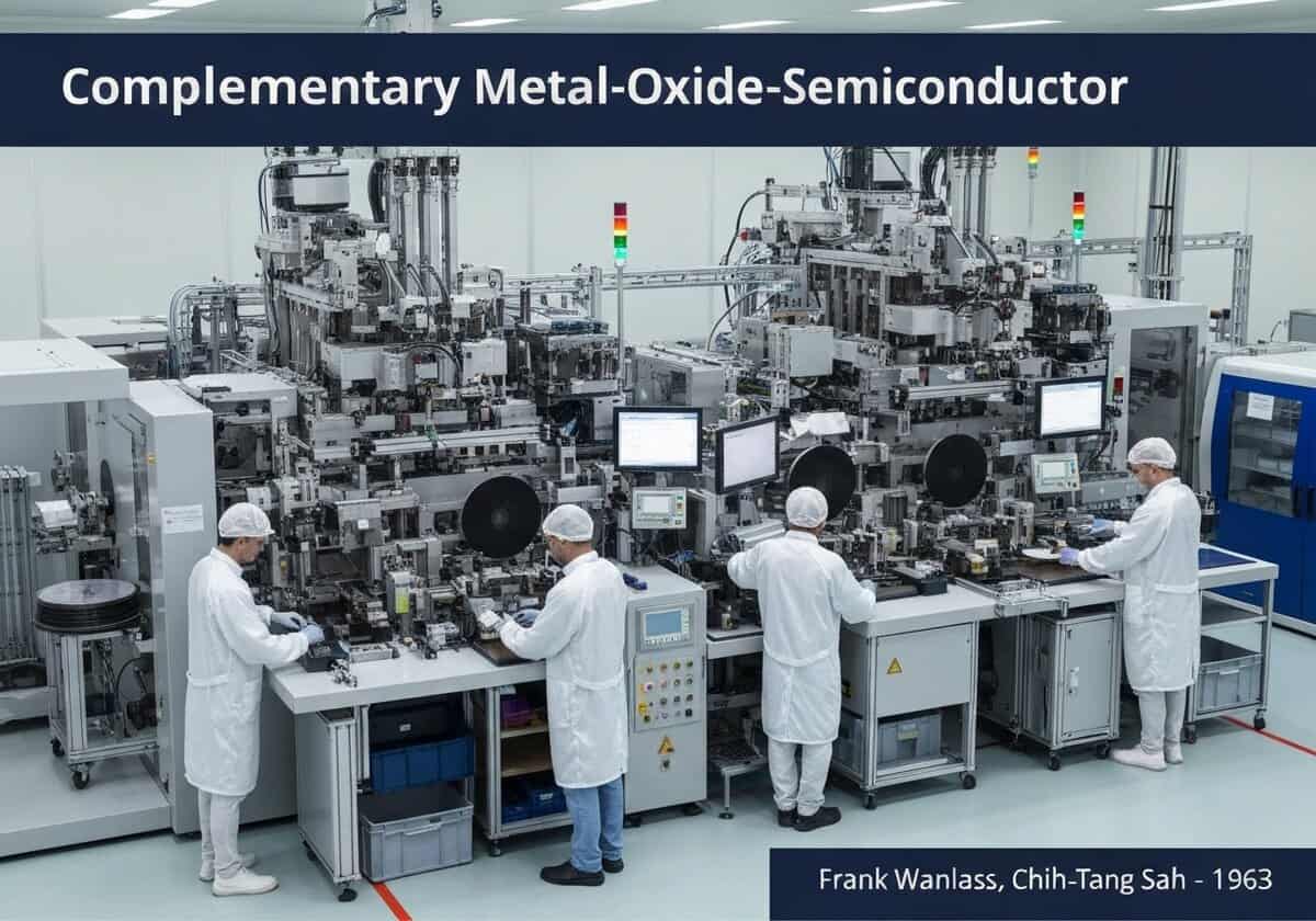
Modern semiconductor fabrication facility focusing on CMOS technology and processes.

(画像はイメージです)

CMOS(相補型金属酸化膜半導体)は、集積回路を構築するための主要な技術です。p型とn型のMOSFETの相補的なペアを使用して論理ゲートを構築します。その主な利点は、静的消費電力が非常に低いことです。 トランジスタ 定常状態では、このペアのスイッチは常にオフになっているため、スイッチング遷移時を除いて電流の流れは最小限に抑えられます。

A CMOS logic gate, such as an inverter, is constructed with both a PMOS (p-type) and an NMOS (n-type) トランジスタ. The PMOS transistor is connected to the positive voltage supply (Vdd), and the NMOS transistor is connected to ground (GND). Their gates are tied together as the input, and their drains are tied together as the output. When the input is low (logic 0), the PMOS transistor turns on, and the NMOS turns off, pulling the output high to Vdd (logic 1). Conversely, when the input is high (logic 1), the PMOS turns off, and the NMOS turns on, pulling the output low to GND (logic 0).

安定状態(出力がハイまたはロー)では、トランジスタの1つがオフになり、電源とグランド間の抵抗値が非常に高くなります。つまり、電流はほとんど流れず、静的消費電力は極めて低くなります。電力は主にトランジスタの状態が切り替わるときに消費されます。この特性により、CMOS技術はバッテリー駆動デバイスや、放熱管理が重要な課題となる高密度集積回路の製造に理想的なものとなりました。世代を重ねるごとにトランジスタの小型化と高速化が進むCMOSのスケーラビリティは、ムーアの法則とデジタル革命の原動力となっています。

UNESCO Nomenclature: 2205
電子機器

タイプ

物理デバイス

混乱

革命的

使用法

広く普及している

前駆物質

  • MOSFETの発明
  • p型およびn型半導体ドーピングの開発
  • トランジスタ製造のための平面プロセス
  • 集積回路の発明

アプリケーション

  • マイクロプロセッサ
  • マイクロコントローラ
  • スタティックRAM(SRAM)
  • イメージセンサー
  • 最新のデジタルロジック回路

特許:

  • US3356858

潜在的なイノベーションのアイデア

  • sub-threshold cmos circuits for ultra-low-power iot devices
  • cmos image sensors for digital cameras and smartphones
  • silicon-on-insulator (soi) cmos for improved performance and radiation hardness
  • 3d cmos integration for stacking multiple circuit layers vertically
  • 極低温 cmos for quantum computer control interfaces
  • cmos-compatible メムズ (micro-electro-mechanical systems)
  • finfet and gate-all-around (gaa) transistors as evolutions of cmos
  • cmos-based biosensors for medical diagnostics
関連キーワード:CMOS、MOSFET、集積回路、低消費電力、半導体、デジタルロジック、マイクロプロセッサ、トランジスタ。

歴史的背景

相補型金属酸化膜半導体(CMOS)

1960
1960-05-16
1962
1963
1964
1968
1970
1960
1960
1961
1962
1963
1965
1970
1970

(日付が不明または関連性がない場合、例えば「流体力学」などでは、その注目すべき出現時期の概算値が提示されます。)

10年目 周年

フルサイズの画像とダウンロードは、登録会員のみが100%無料で利用できます。