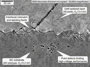
I semiconduttori a banda proibita ampia, principalmente carburo di silicio (SiC) e nitruro di gallio (GaN), supportano campi elettrici, temperature di giunzione e frequenze di commutazione più elevati rispetto al silicio. Le bande proibite di circa 3,3 eV per il 4H-SiC e 3,4 eV per il GaN riducono le perdite di conduzione e di commutazione. Permettono inoltre di ridurre le dimensioni dei componenti passivi e dei sistemi di raffreddamento. I MOSFET in SiC dominano gli inverter di trazione e i caricabatterie ad alta tensione. Gli HEMT in GaN sono leader nei convertitori compatti, dagli alimentatori industriali a 650 V fino agli adattatori per uso domestico e ai sistemi di alimentazione per data center.
Diversi problemi ne limitano ancora l'adozione. Il SiC soffre di difetti del substrato, costi elevati per la crescita dei wafer e affidabilità dell'ossido di gate. Il GaN presenta problemi di resistenza dinamica di conduzione, instabilità della tensione di soglia e assenza di substrati nativi economici, il che spinge verso l'eteroepitassia GaN su silicio. I dispositivi a ossido di gallio e GaN verticale sono progettati per tensioni più elevate. L'uso in ambito automobilistico è vincolato dalla qualificazione secondo le linee guida AEC-Q101 e JEDEC. Le pubblicazioni e i brevetti indicizzati di seguito riguardano le strutture dei dispositivi, l'epitassia e la lavorazione dei wafer, i driver di gate, il packaging dei moduli e i test di affidabilità.
SiC e GaN commutano più velocemente e funzionano a temperature più elevate rispetto al silicio, motivo per cui dominano l'elettronica di potenza moderna. Le sfide di packaging sono in corso imballaggio avanzatoe l'industria generale è in funzione semiconduttoriI clienti tipici compaiono in reti intelligenti E pannelli solariLa crescita dei cristalli è in corso deposizione di vapore chimico.
Questa è la nostra ultima selezione di pubblicazioni e brevetti mondiali in inglese sui semiconduttori a banda larga (SiC e GaN), provenienti da numerose riviste scientifiche online, classificate e focalizzate su semiconduttori a banda larga, carburo di silicio, MOSFET SiC, moduli di potenza SiC, wafer SiC, 4H-SiC, epitassia del carburo di silicio, nitruro di gallio, HEMT GaN, GaN su silicio, GaN verticale, ossido di gallio, affidabilità dell'ossido di gate, instabilità della tensione di soglia, gate a trincea, diodo di corpo, inverter di trazione e caricabatterie di bordo.
Euv reflector
Patent published on the 2026-11-11 in EP under Ref EP4838269 by ZEISS CARL SMT GMBH [DE] (Blauw Michiel Alexander [nl], Van De Kerkhof Marcus Adrianus [nl])
Abstract: [0001] An EUV reflector comprising a ruthenium capping layer, a molybdenum silicon multilayer and a bilayer comprising an upper layer and a lower layer. The bilayer is positioned between the capping layer and the multilayer. The upper layer comprises carbon, boron, boron carbide, silicon, molybdenum and/or mixtures thereof. The lower layer comprises silicon nitride, amorphous carbon, diamond-like carbon, silicon carbide, boron nitride and/or mixtures thereof.[...]
Our summary: The EUV reflector features a ruthenium capping layer and a molybdenum silicon multilayer. It includes a bilayer with an upper layer made of various materials and a lower layer composed of silicon nitride and other compounds. This design enhances the performance of the reflector in extreme ultraviolet applications.
EUV reflector, ruthenium capping layer, molybdenum silicon multilayer, bilayer
Patent
Poly-sic wafer with structural features and heat transfer characteristics
Patent published on the 2026-11-05 in WO under Ref WO2026231181 by MICROCHIP TECH INCORPORATED [US] (Nagel Steve [us], Chen Bomy [us])
Abstract: A method provides a silicon wafer having a front side and a back side, shapes the silicon wafer to have a silicon base at the back side and a silicon mandrel having a proximal end at the silicon base and a distal end at the front side, forms a ceramic wafer comprising the silicon wafer having the silicon mandrel, removes the silicon mandrel from the ceramic wafer to form a feature in a front side of the ceramic wafer, provides a donor silicon wafer having a front side and a back side, and bonds [...]
Our summary: A method creates a poly-sic wafer with distinct structural features for enhanced heat transfer. It involves shaping a silicon wafer and forming a ceramic wafer with a silicon mandrel. The process concludes with bonding a donor silicon wafer to the ceramic wafer.
poly-sic wafer, heat transfer, silicon mandrel, ceramic wafer
Patent
Polysic wafer base with mandrel defined power and ground rails
Patent published on the 2026-11-05 in WO under Ref WO2026231182 by MICROCHIP TECH INCORPORATED [US] (Nagel Steve [us], Chen Bomy [us])
Abstract: A method provides a silicon wafer shaped to have a silicon base at the backside and a silicon mandrel at the frontside, forming a ceramic wafer with silicon mandrel, removing the silicon mandrel from the ceramic wafer to form a feature in a frontside of the ceramic wafer, and inputting a conductive material in the feature to form a backside power line. A system has a ceramic wafer of SiC powder heated and pressed into an amorphous poly-SiC ceramic, a power line and a power rail in the backside o[...]
Our summary: A method describes creating a ceramic wafer with a silicon mandrel and backside power lines. The silicon mandrel is removed to form features for conductive material input. A system integrates a ceramic wafer with power rails and a semiconductor package.
Polysilicon, Ceramic Wafer, Semiconductor Package, Power Rails
Patent
Poly-sic wafer with structural features and heat transfer characteristics
Patent published on the 2026-11-05 in US under Ref US20260354131 by MICROCHIP TECH INC [US] (Nagel Steve [us], Chen Bomy [us])
Abstract: [0000] A method provides a silicon wafer having a front side and a back side, shapes the silicon wafer to have a silicon base at the back side and a silicon mandrel having a proximal end at the silicon base and a distal end at the front side, forms a ceramic wafer comprising the silicon wafer having the silicon mandrel, removes the silicon mandrel from the ceramic wafer to form a feature in a front side of the ceramic wafer, provides a donor silicon wafer having a front side and a back side, and[...]
Our summary: The method describes creating a silicon wafer with a specific structure for enhanced heat transfer. It involves shaping the wafer and forming a ceramic layer with a silicon mandrel. Finally, a donor silicon wafer is bonded to the ceramic wafer to complete the process.
Poly-sic, silicon wafer, heat transfer, ceramic wafer
Patent
Stacked thermal interface components comprising high thermal conductivity layers for semiconductor packaging
Patent published on the 2026-10-29 in US under Ref US20260344426 by ENTEGRIS INC [US] (Mahadev Niraj [us], Singh Rajiv K [us], Verma Aditya Dilip [us], De Sunny [us], Alety Sridevi R [us])
Abstract: [0000] A thermal interface component for a semiconductor device packaging structure includes a first layer comprising a thermal interface material having a thermal conductivity of at least 200 W·m·Kand a second layer having a thermal conductivity from 0.1% to 80% of the thermal conductivity of the first layer. The first layer is supported by the second layer, and a thickness of the first layer is greater than a thickness of the second layer. The thermal interface component is dimensioned for i[...]
Our summary: This content describes a thermal interface component for semiconductor packaging with a high thermal conductivity first layer. The first layer is supported by a second layer with lower thermal conductivity. The design allows for integration into semiconductor devices, potentially including additional layers for enhanced performance.
thermal interface materials, semiconductor packaging, thermal conductivity, layered structures
Patent
Ceramic matrix composites
Patent published on the 2026-10-28 in GB under Ref GB2705710 by UNITED KINGDOM ATOMIC ENERGY AUTHORITY [GB] (James Wade-zhu [gb], Virtudes Rubio [gb])
Abstract: A method 100 for forming a non-oxide ceramic matrix composite (CMC) comprising; impregnating a plurality of fibres of non-oxide material with a slurry comprising non-oxide powder by drawing the plurality of fibres through the slurry 102, forming a pre-ceramic composition by pressure infiltrating the impregnated fibres with a fluid polymer and cross-linking under pressure 108, and heat treating 110 the pre-ceramic composition to form the non-oxide CMC. Drawing the plurality of fibres through the [...]
Our summary: This method forms a non-oxide ceramic matrix composite by impregnating fibres with a slurry of non-oxide powder. The process involves pressure infiltrating the fibres with a fluid polymer and cross-linking them. Finally, the pre-ceramic composition is heat treated to create the non-oxide CMC.
Ceramic matrix composites, non-oxide materials, heat treatment, polymer infiltration
Patent
Highly Sensitive Room-Temperature Graphene-Modulated AlGaN/GaN HEMT THz Detector Architecture
Published on 2026-02-03 by Rudrarup Sengupta, Gabby Sarusi @MDPI
Abstract: This work proposes new architecture, supported by analytical modelling and computer-aided design (CAD) simulations, for a highly sensitive monolayer graphene-gated AlGaN/GaN HEMT terahertz (THz) detector operating at room temperature (RT). The monolayer graphene gate acts as a surface plasmon absorber for the incident THz radiation. The carrier density perturbation caused by incident THz energy on the monolayer graphene surface is then capacitively coupled to the two-dimensional electron gas (2D[...]
Our summary: This work presents a novel architecture for a room-temperature AlGaN/GaN HEMT THz detector utilizing a monolayer graphene gate. The graphene gate enhances sensitivity by acting as a surface plasmon absorber, allowing for effective carrier density modulation. Simulations indicate a high responsivity of 2.12 × 10^6 V/W at 1 THz with a broadband bandwidth of 2 THz.
Graphene, HEMT, THz detector, room temperature
Publication
Processing Characteristics of Ultra-Precision Cutting of 4H-SiC Wafers by Dicing Blade
Published on 2026-01-30 by Yufang Wang, Zhixiong Li, Fengjun Chen, Zhiqiang Xu @MDPI
Abstract: Dicing is an important process in the packaging segment of the semiconductor manufacturing process, and due to the high hardness and brittleness of 4H-SiC wafers, they are prone to crack propagation and severe chipping during the dicing process. To reduce chipping defects, this study investigates the effects of key process parameters on the chipping behavior of 4H-SiC wafers, as well as the associated chipping formation and material removal mechanisms during dicing. Firstly, a spindle current me[...]
Our summary: This study explores the effects of process parameters on chipping behavior during the dicing of 4H-SiC wafers. It utilizes spindle current measurements to analyze grinding force changes and identifies optimal cutting parameters to reduce defects. Additionally, it investigates chipping formation and material removal mechanisms to enhance understanding and optimization of the cutting process.
Dicing, 4H-SiC, Chipping, Cutting Process
Publication