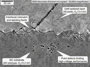
주로 탄화규소(SiC)와 질화갈륨(GaN)으로 대표되는 넓은 밴드갭 반도체는 실리콘보다 높은 전기장, 접합 온도 및 스위칭 주파수를 견딜 수 있습니다. 4H-SiC의 경우 약 3.3eV, GaN의 경우 약 3.4eV의 밴드갭은 전도 손실과 스위칭 손실을 줄여줍니다. 또한 수동 부품과 냉각 장치의 크기를 줄여줍니다. SiC MOSFET은 자동차용 인버터와 고전압 충전기에 주로 사용됩니다. GaN HEMT는 650V 산업용 전원 공급 장치부터 소비자용 어댑터 및 데이터 센터 전원 랙에 이르기까지 소형 컨버터 분야에서 널리 사용됩니다.
여전히 여러 가지 문제가 상용화를 제한하고 있습니다. SiC는 기판 결함, 고비용의 웨이퍼 성장, 게이트 산화막 신뢰성 문제를 안고 있습니다. GaN은 동적 온 저항, 문턱 전압 불안정성, 저렴한 네이티브 기판의 부재로 인해 GaN-on-silicon 이종 에피택시 기술이 주목받고 있습니다. 산화갈륨 및 수직형 GaN 소자는 더 높은 전압을 목표로 합니다. 자동차 분야에서의 사용은 AEC-Q101 및 JEDEC 가이드라인에 따른 인증을 통해 제한됩니다. 아래에 색인된 논문 및 특허는 소자 구조, 에피택시 및 웨이퍼 공정, 게이트 드라이버, 모듈 패키징 및 신뢰성 테스트를 다룹니다.
SiC와 GaN은 실리콘보다 스위칭 속도가 빠르고 발열량이 높아 현대 전력 전자 분야에서 지배적인 위치를 차지하고 있습니다. 하지만 패키징 문제는 여전히 해결해야 할 과제입니다. 고급 포장그리고 일반 산업은 반도체일반적인 고객은 다음과 같습니다. 스마트 그리드 그리고 태양광 패널결정 성장이 진행 중입니다. 화학 기상 증착.
본 자료는 광대역 반도체(SiC 및 GaN)에 관한 전 세계 영문 논문 및 특허를 엄선하여 정리한 것으로, 다양한 온라인 과학 저널에 게재된 자료들을 포함하고 있습니다. 주요 주제는 광대역 반도체, 탄화규소, SiC MOSFET, SiC 전력 모듈, SiC 웨이퍼, 4H-SiC, 탄화규소 에피택시, 질화갈륨, GaN HEMT, GaN-on-silicon, 수직형 GaN, 산화갈륨, 게이트 산화막 신뢰성, 임계 전압 불안정성, 트렌치 게이트, 바디 다이오드, 트랙션 인버터 및 온보드 충전기입니다.
Euv reflector
Patent published on the 2026-11-11 in EP under Ref EP4838269 by ZEISS CARL SMT GMBH [DE] (Blauw Michiel Alexander [nl], Van De Kerkhof Marcus Adrianus [nl])
Abstract: [0001] An EUV reflector comprising a ruthenium capping layer, a molybdenum silicon multilayer and a bilayer comprising an upper layer and a lower layer. The bilayer is positioned between the capping layer and the multilayer. The upper layer comprises carbon, boron, boron carbide, silicon, molybdenum and/or mixtures thereof. The lower layer comprises silicon nitride, amorphous carbon, diamond-like carbon, silicon carbide, boron nitride and/or mixtures thereof.[...]
Our summary: The EUV reflector features a ruthenium capping layer and a molybdenum silicon multilayer. It includes a bilayer with an upper layer made of various materials and a lower layer composed of silicon nitride and other compounds. This design enhances the performance of the reflector in extreme ultraviolet applications.
EUV reflector, ruthenium capping layer, molybdenum silicon multilayer, bilayer
Patent
Poly-sic wafer with structural features and heat transfer characteristics
Patent published on the 2026-11-05 in WO under Ref WO2026231181 by MICROCHIP TECH INCORPORATED [US] (Nagel Steve [us], Chen Bomy [us])
Abstract: A method provides a silicon wafer having a front side and a back side, shapes the silicon wafer to have a silicon base at the back side and a silicon mandrel having a proximal end at the silicon base and a distal end at the front side, forms a ceramic wafer comprising the silicon wafer having the silicon mandrel, removes the silicon mandrel from the ceramic wafer to form a feature in a front side of the ceramic wafer, provides a donor silicon wafer having a front side and a back side, and bonds [...]
Our summary: A method creates a poly-sic wafer with distinct structural features for enhanced heat transfer. It involves shaping a silicon wafer and forming a ceramic wafer with a silicon mandrel. The process concludes with bonding a donor silicon wafer to the ceramic wafer.
poly-sic wafer, heat transfer, silicon mandrel, ceramic wafer
Patent
Polysic wafer base with mandrel defined power and ground rails
Patent published on the 2026-11-05 in WO under Ref WO2026231182 by MICROCHIP TECH INCORPORATED [US] (Nagel Steve [us], Chen Bomy [us])
Abstract: A method provides a silicon wafer shaped to have a silicon base at the backside and a silicon mandrel at the frontside, forming a ceramic wafer with silicon mandrel, removing the silicon mandrel from the ceramic wafer to form a feature in a frontside of the ceramic wafer, and inputting a conductive material in the feature to form a backside power line. A system has a ceramic wafer of SiC powder heated and pressed into an amorphous poly-SiC ceramic, a power line and a power rail in the backside o[...]
Our summary: A method describes creating a ceramic wafer with a silicon mandrel and backside power lines. The silicon mandrel is removed to form features for conductive material input. A system integrates a ceramic wafer with power rails and a semiconductor package.
Polysilicon, Ceramic Wafer, Semiconductor Package, Power Rails
Patent
Poly-sic wafer with structural features and heat transfer characteristics
Patent published on the 2026-11-05 in US under Ref US20260354131 by MICROCHIP TECH INC [US] (Nagel Steve [us], Chen Bomy [us])
Abstract: [0000] A method provides a silicon wafer having a front side and a back side, shapes the silicon wafer to have a silicon base at the back side and a silicon mandrel having a proximal end at the silicon base and a distal end at the front side, forms a ceramic wafer comprising the silicon wafer having the silicon mandrel, removes the silicon mandrel from the ceramic wafer to form a feature in a front side of the ceramic wafer, provides a donor silicon wafer having a front side and a back side, and[...]
Our summary: The method describes creating a silicon wafer with a specific structure for enhanced heat transfer. It involves shaping the wafer and forming a ceramic layer with a silicon mandrel. Finally, a donor silicon wafer is bonded to the ceramic wafer to complete the process.
Poly-sic, silicon wafer, heat transfer, ceramic wafer
Patent
Stacked thermal interface components comprising high thermal conductivity layers for semiconductor packaging
Patent published on the 2026-10-29 in US under Ref US20260344426 by ENTEGRIS INC [US] (Mahadev Niraj [us], Singh Rajiv K [us], Verma Aditya Dilip [us], De Sunny [us], Alety Sridevi R [us])
Abstract: [0000] A thermal interface component for a semiconductor device packaging structure includes a first layer comprising a thermal interface material having a thermal conductivity of at least 200 W·m·Kand a second layer having a thermal conductivity from 0.1% to 80% of the thermal conductivity of the first layer. The first layer is supported by the second layer, and a thickness of the first layer is greater than a thickness of the second layer. The thermal interface component is dimensioned for i[...]
Our summary: This content describes a thermal interface component for semiconductor packaging with a high thermal conductivity first layer. The first layer is supported by a second layer with lower thermal conductivity. The design allows for integration into semiconductor devices, potentially including additional layers for enhanced performance.
thermal interface materials, semiconductor packaging, thermal conductivity, layered structures
Patent
Ceramic matrix composites
Patent published on the 2026-10-28 in GB under Ref GB2705710 by UNITED KINGDOM ATOMIC ENERGY AUTHORITY [GB] (James Wade-zhu [gb], Virtudes Rubio [gb])
Abstract: A method 100 for forming a non-oxide ceramic matrix composite (CMC) comprising; impregnating a plurality of fibres of non-oxide material with a slurry comprising non-oxide powder by drawing the plurality of fibres through the slurry 102, forming a pre-ceramic composition by pressure infiltrating the impregnated fibres with a fluid polymer and cross-linking under pressure 108, and heat treating 110 the pre-ceramic composition to form the non-oxide CMC. Drawing the plurality of fibres through the [...]
Our summary: This method forms a non-oxide ceramic matrix composite by impregnating fibres with a slurry of non-oxide powder. The process involves pressure infiltrating the fibres with a fluid polymer and cross-linking them. Finally, the pre-ceramic composition is heat treated to create the non-oxide CMC.
Ceramic matrix composites, non-oxide materials, heat treatment, polymer infiltration
Patent
Highly Sensitive Room-Temperature Graphene-Modulated AlGaN/GaN HEMT THz Detector Architecture
Published on 2026-02-03 by Rudrarup Sengupta, Gabby Sarusi @MDPI
Abstract: This work proposes new architecture, supported by analytical modelling and computer-aided design (CAD) simulations, for a highly sensitive monolayer graphene-gated AlGaN/GaN HEMT terahertz (THz) detector operating at room temperature (RT). The monolayer graphene gate acts as a surface plasmon absorber for the incident THz radiation. The carrier density perturbation caused by incident THz energy on the monolayer graphene surface is then capacitively coupled to the two-dimensional electron gas (2D[...]
Our summary: This work presents a novel architecture for a room-temperature AlGaN/GaN HEMT THz detector utilizing a monolayer graphene gate. The graphene gate enhances sensitivity by acting as a surface plasmon absorber, allowing for effective carrier density modulation. Simulations indicate a high responsivity of 2.12 × 10^6 V/W at 1 THz with a broadband bandwidth of 2 THz.
Graphene, HEMT, THz detector, room temperature
Publication
Processing Characteristics of Ultra-Precision Cutting of 4H-SiC Wafers by Dicing Blade
Published on 2026-01-30 by Yufang Wang, Zhixiong Li, Fengjun Chen, Zhiqiang Xu @MDPI
Abstract: Dicing is an important process in the packaging segment of the semiconductor manufacturing process, and due to the high hardness and brittleness of 4H-SiC wafers, they are prone to crack propagation and severe chipping during the dicing process. To reduce chipping defects, this study investigates the effects of key process parameters on the chipping behavior of 4H-SiC wafers, as well as the associated chipping formation and material removal mechanisms during dicing. Firstly, a spindle current me[...]
Our summary: This study explores the effects of process parameters on chipping behavior during the dicing of 4H-SiC wafers. It utilizes spindle current measurements to analyze grinding force changes and identifies optimal cutting parameters to reduce defects. Additionally, it investigates chipping formation and material removal mechanisms to enhance understanding and optimization of the cutting process.
Dicing, 4H-SiC, Chipping, Cutting Process
Publication