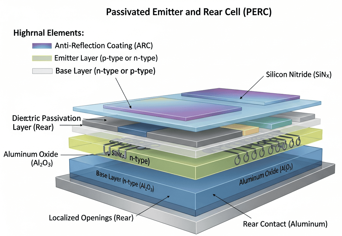

钝化发射极和背接触(PERC)技术通过在背面硅表面引入介电钝化层(通常为覆盖有SiNx的Al2O3),扩展了传统的铝背表面场太阳能电池,从而抑制复合并提高内部背面反射率。性能提升源于表面复合速度的降低、少数载流子寿命的延长以及通过激光烧蚀形成的优化局部背面接触。
工艺集成旨在解决PECVD或ALD沉积均匀性、丝网印刷金属化、烧结曲线和氢钝化动力学等问题。光致硼氧缺陷引起的性能退化及其通过再生退火的缓解仍然是当前研究的热点。
本页面汇总了最新的同行评审出版物和已授权专利,内容涵盖 PERC 电池物理、制造工艺、双面变体和组件级集成:
这是我们最新精选的全球英文出版物和专利,涵盖钝化发射极和背接触 (PERC) 的众多科学在线期刊,并按以下主题进行分类和重点介绍:背面钝化、氧化铝钝化、氮化硅钝化、局部背接触、激光接触开口、介电钝化层、表面复合速度、少数载流子寿命、背面反射率、内部量子效率、双面 PERC、PERC+、背发射极、正面场、选择性发射极、氢钝化、烧结工艺、Al2O3 沉积、PECVD 沉积、ALD 沉积、背面激光烧蚀、接触电阻、填充因子优化、光致退化、硼氧缺陷、再生退火、吸杂工艺、体缺陷钝化、开路电压增强、丝网印刷金属化以及钝化发射极和背接触。
Thermoelectric conversion member, production method for same, and thermoelectric conversion element
Patent published on the 2026-05-28 in WO under Ref WO2026110560 by NATIONAL INST FOR MATERIALS SCIENCE [JP] (Mori Takao [jp], Li Airan [jp])
Abstract: The present invention provides: a thermoelectric conversion member that makes it possible to reduce contact resistance between a MgAgSb-based thermoelectric material and an electrode; a production method for the same; and a thermoelectric conversion element. A thermoelectric conversion member according to the present invention comprises at least: a thermoelectric conversion layer which comprises a p-type thermoelectric material that includes magnesium (Mg), silver (Ag), and antimony (Sb); and [...]
Our summary: The invention presents a thermoelectric conversion member that reduces contact resistance between a MgAgSb-based material and an electrode. It includes a p-type thermoelectric layer and an Sb layer on its end surface. The production method involves forming and sintering a laminate of raw materials for the thermoelectric material and the Sb layer.
thermoelectric conversion, contact resistance, production method, MgAgSb
Patent
Photovoltaic cell preparation method and photovoltaic cell
Patent published on the 2026-05-27 in EP under Ref EP4750273 by ZHEJIANG JINKO SOLAR CO LTD [CN] (Zeng Xianhuan [cn], Wang Yilan [cn], Li Chao [cn], Zhang Ning [cn])
Abstract: The present disclosure relates to a photovoltaic cell preparation method, and a photovoltaic cell. The method includes: preparing a substrate including a first surface and a second surface opposite to each other, wherein the first surface is a textured structure; placing the substrate into an ALD deposition chamber; sequentially depositing an aluminum-silicon layer and an alumina layer on the first surface; placing the substrate having the aluminum-silicon layer and the alumina layer into a PECV[...]
Our summary: The disclosure presents a method for preparing photovoltaic cells. It involves depositing aluminum-silicon and alumina layers, followed by a silicon nitride layer using PECVD. This process enhances the cell s efficiency by reducing damage from ultraviolet light through improved chemical bonding.
Photovoltaic cell, ALD deposition, PECVD deposition, conversion efficiency
Patent
Semiconductor device and manufacturing method based on seedless silicon source/drain contact resistance reduction and laser process technology
Patent published on the 2026-04-23 in US under Ref US20260114019 by KOREA UNIV RESEARCH AND BUSINESS FOUNDATION [KR] (Yu Hyun-yong [kr], Park Jongyoun [kr], Park Euyjin [kr], Ahn Choong-hyun [kr], Lee Sangsu [kr])
Abstract: [0000] Disclosed are a semiconductor device based on seedless silicon (Si) source/drain contact resistance reduction and laser process technology and a method of fabricating the same. The semiconductor device includes an activated seedless Si layer formed on a substrate and at least one electrode formed on the seedless Si layer, and the seedless Si layer is crystalized through a first laser process and then activated through a second laser process.[...]
Our summary: The invention relates to a semiconductor device utilizing seedless silicon for reduced source/drain contact resistance. It involves a method of fabrication that includes a first laser process for crystallization and a second laser process for activation. The device features an activated seedless silicon layer on a substrate with at least one electrode.
Semiconductor, Seedless Silicon, Contact Resistance, Laser Process
Patent
Connector terminal, electrical connection assembly and connector
Patent published on the 2026-04-15 in EP under Ref EP4726932 by TYCO ELECTRONICS TECH SIP LTD [CN] (Du Yu [cn], Pan Lei [cn], Zhang Weidong [cn])
Abstract: [0001] The present invention discloses a connector terminal, an electrical connection assembly, and a connector. The connector terminal comprises: a terminal body and an elastic component. The terminal body includes: a mating part which has an insertion cavity that allows a mating terminal to be inserted and a first spring arm protruding into the insertion cavity. The elastic component is fixed to the mating part and has a second spring arm protruding into the insertion cavity. The elastic compo[...]
Our summary: The invention involves a connector terminal featuring a terminal body and an elastic component. The elastic component enhances electrical contact by clamping a mating terminal with its spring arms. It also improves insertion ease and contact resistance due to its material properties.
connector terminal, electrical connection, assembly, elastic component
Patent
External control of photocleavage reactivity in polymer networks to reconcile photodegradability and photostability
Published on 2026-04-13 by Hiroshi Masai @NATURE
Abstract: Polymer Journal, Published online: 13 April 2026; doi:10.1038/s41428-026-01165-6This review summarizes our recent strategies for controlling the photostability and photoreactivity of polymer materials. Beyond conventional photoreactive polymers, we have developed polymer systems that exhibit cooperative reactions triggered by combined light and acid stimuli, as well as tunable photoreactivity based on reversible intramolecular isomerization. These systems show significant promise for a wide rang[...]
Our summary: This review discusses strategies for controlling the photostability and photoreactivity of polymer materials. It highlights the development of polymer systems that respond to combined light and acid stimuli. The findings suggest potential applications in light-induced degradation and processing in light-irradiated environments.
photocleavage, photostability, polymer networks, photoreactivity
Publication
Method of manufacturing point contact solar cells and apparatus using the same
Patent published on the 2026-04-09 in US under Ref US20260101606 by TERASOLAR ENERGY MAT CORP [TW] (Wu Pang-hao [tw], Lin Shih-cheng [tw], Tang Cheng-syun [tw])
Abstract: [0000] A method of manufacturing high-efficiency solar cells by reducing contact resistance and forming point-contacts is disclosed. The method includes providing a silicon substrate with a metallic electrode on its surface, and applying a high-frequency pulsed voltage comprised of pulse-on time and pulse-off time to the metallic electrode. The method further includes illuminating the silicon substrate using a laser and scanning the substrate under the high-frequency pulsed voltage. During the p[...]
Our summary: A method for manufacturing high-efficiency solar cells involves reducing contact resistance through point-contacts. It utilizes a silicon substrate with a metallic electrode, applying a high-frequency pulsed voltage and laser illumination. The process thermally inter-diffuses metal and silicon to create separate contact regions.
solar cells, point contact, silicon substrate, high-frequency pulsed voltage
Patent
In-plane controllably grown germanium nanowire, preparation method therefor, and use thereof
Patent published on the 2026-03-26 in WO under Ref WO2026061089 by INST OF PHYSICS CHINESE ACADEMY OF SCIENCES [CN] (Wang Jianhuan [cn], Zhang Jianjun [cn], Xu Hongqi [cn])
Abstract: Disclosed in the present application are an in-plane controllably grown germanium nanowire, a preparation method therefor, and the use thereof. The method comprises: obtaining a strip-shaped platform structure on a silicon germanium substrate; pretreating the silicon germanium substrate having the strip-shaped platform structure; and using a molecular beam epitaxy growth technique to sequentially grow a silicon germanium buffer layer, a silicon spacer layer, a pure germanium layer and a silicon [...]
Our summary: The application discloses a method for preparing in-plane controllably grown germanium nanowires. It involves a silicon germanium substrate and molecular beam epitaxy to create multiple layers. This method overcomes high contact resistance and improves material mobility, benefiting quantum dot devices and spin bits.
germanium nanowire, molecular beam epitaxy, silicon germanium substrate, quantum dot devices
Patent
Thermographic Diagnosis of Corrosion-Driven Contact Degradation in Power Equipment Using Infrared Imaging and Color-Channel Decomposition
Published on 2026-02-01 by Milton Ruiz, Carlos Betancourt @MDPI
Abstract: This study presents a measurement–modeling pathway for diagnosing corrosion-driven contact degradation in power equipment using infrared thermography and color-channel analysis. Thermal data were acquired with a Fluke Ti450 (LWIR, 7.5–14 μm) under typical high-altitude, temperate conditions in Quito, Ecuador. Radiometric parameters (emissivity, distance, ambient/reflected temperature, and humidity) are reported explicitly, and images are processed with a re[...]
Our summary: This study outlines a method for diagnosing corrosion-driven contact degradation in power equipment using infrared thermography and color-channel analysis. Thermal data were collected in Quito, Ecuador, with a focus on radiometric parameters and image processing techniques. The approach is validated through field cases, emphasizing the importance of clear radiometric practices for effective maintenance decisions.
Thermography, Corrosion, Infrared Imaging, Power Equipment
Publication