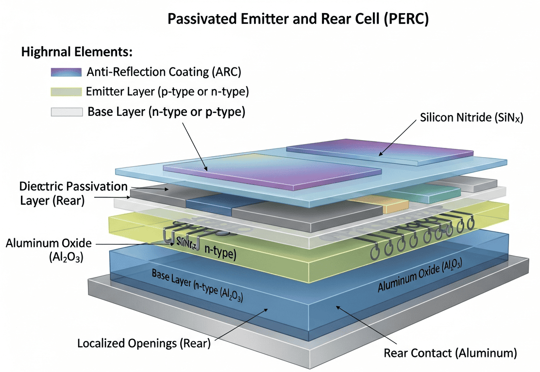

A tecnologia PERC (Passivated Emitter and Rear Cell) amplia as capacidades das células solares convencionais de alumínio com campo de superfície traseira, introduzindo uma camada de passivação dielétrica — tipicamente Al2O3 revestida com SiNx — na superfície traseira de silício. Essa camada suprime a recombinação e aumenta a refletância interna traseira. Os ganhos de desempenho derivam da redução da velocidade de recombinação superficial, do aumento da vida útil dos portadores minoritários e da otimização dos contatos traseiros locais abertos por ablação a laser.
A integração de processos aborda a uniformidade da deposição por PECVD ou ALD, a metalização por serigrafia, os perfis de queima e a dinâmica da passivação por hidrogênio. A degradação induzida pela luz devido a defeitos de boro-oxigênio e sua mitigação por meio de recozimento regenerativo continuam sendo um foco ativo de pesquisa.
Esta página reúne as publicações revisadas por pares mais recentes e as patentes concedidas que abrangem a física das células PERC, processos de fabricação, variantes bifaciais e integração em nível de módulo:
Esta é a nossa mais recente seleção de publicações e patentes mundiais em inglês sobre Célula de Emissor e Traseiro Passivados (PERC), provenientes de diversos periódicos científicos online, classificadas e focadas em passivação da superfície traseira, passivação com óxido de alumínio, passivação com nitreto de silício, contato traseiro local, abertura de contato a laser, camada de passivação dielétrica, velocidade de recombinação superficial, tempo de vida do portador minoritário, refletância traseira, eficiência quântica interna, PERC bifacial, PERC+, emissor traseiro, campo de superfície frontal, emissor seletivo, passivação por hidrogênio, processo de queima, deposição de Al2O3, deposição por PECVD, deposição por ALD, ablação a laser traseira, resistência de contato, otimização do fator de preenchimento, degradação induzida por luz, defeito boro-oxigênio, recozimento de regeneração, processo de getterização, passivação de defeitos em massa, aumento da tensão de circuito aberto, metalização por serigrafia e Célula de Emissor e Traseiro Passivados.
Thermoelectric conversion member, production method for same, and thermoelectric conversion element
Patent published on the 2026-05-28 in WO under Ref WO2026110560 by NATIONAL INST FOR MATERIALS SCIENCE [JP] (Mori Takao [jp], Li Airan [jp])
Abstract: The present invention provides: a thermoelectric conversion member that makes it possible to reduce contact resistance between a MgAgSb-based thermoelectric material and an electrode; a production method for the same; and a thermoelectric conversion element. A thermoelectric conversion member according to the present invention comprises at least: a thermoelectric conversion layer which comprises a p-type thermoelectric material that includes magnesium (Mg), silver (Ag), and antimony (Sb); and [...]
Our summary: The invention presents a thermoelectric conversion member that reduces contact resistance between a MgAgSb-based material and an electrode. It includes a p-type thermoelectric layer and an Sb layer on its end surface. The production method involves forming and sintering a laminate of raw materials for the thermoelectric material and the Sb layer.
thermoelectric conversion, contact resistance, production method, MgAgSb
Patent
Photovoltaic cell preparation method and photovoltaic cell
Patent published on the 2026-05-27 in EP under Ref EP4750273 by ZHEJIANG JINKO SOLAR CO LTD [CN] (Zeng Xianhuan [cn], Wang Yilan [cn], Li Chao [cn], Zhang Ning [cn])
Abstract: The present disclosure relates to a photovoltaic cell preparation method, and a photovoltaic cell. The method includes: preparing a substrate including a first surface and a second surface opposite to each other, wherein the first surface is a textured structure; placing the substrate into an ALD deposition chamber; sequentially depositing an aluminum-silicon layer and an alumina layer on the first surface; placing the substrate having the aluminum-silicon layer and the alumina layer into a PECV[...]
Our summary: The disclosure presents a method for preparing photovoltaic cells. It involves depositing aluminum-silicon and alumina layers, followed by a silicon nitride layer using PECVD. This process enhances the cell s efficiency by reducing damage from ultraviolet light through improved chemical bonding.
Photovoltaic cell, ALD deposition, PECVD deposition, conversion efficiency
Patent
Semiconductor device and manufacturing method based on seedless silicon source/drain contact resistance reduction and laser process technology
Patent published on the 2026-04-23 in US under Ref US20260114019 by KOREA UNIV RESEARCH AND BUSINESS FOUNDATION [KR] (Yu Hyun-yong [kr], Park Jongyoun [kr], Park Euyjin [kr], Ahn Choong-hyun [kr], Lee Sangsu [kr])
Abstract: [0000] Disclosed are a semiconductor device based on seedless silicon (Si) source/drain contact resistance reduction and laser process technology and a method of fabricating the same. The semiconductor device includes an activated seedless Si layer formed on a substrate and at least one electrode formed on the seedless Si layer, and the seedless Si layer is crystalized through a first laser process and then activated through a second laser process.[...]
Our summary: The invention relates to a semiconductor device utilizing seedless silicon for reduced source/drain contact resistance. It involves a method of fabrication that includes a first laser process for crystallization and a second laser process for activation. The device features an activated seedless silicon layer on a substrate with at least one electrode.
Semiconductor, Seedless Silicon, Contact Resistance, Laser Process
Patent
Connector terminal, electrical connection assembly and connector
Patent published on the 2026-04-15 in EP under Ref EP4726932 by TYCO ELECTRONICS TECH SIP LTD [CN] (Du Yu [cn], Pan Lei [cn], Zhang Weidong [cn])
Abstract: [0001] The present invention discloses a connector terminal, an electrical connection assembly, and a connector. The connector terminal comprises: a terminal body and an elastic component. The terminal body includes: a mating part which has an insertion cavity that allows a mating terminal to be inserted and a first spring arm protruding into the insertion cavity. The elastic component is fixed to the mating part and has a second spring arm protruding into the insertion cavity. The elastic compo[...]
Our summary: The invention involves a connector terminal featuring a terminal body and an elastic component. The elastic component enhances electrical contact by clamping a mating terminal with its spring arms. It also improves insertion ease and contact resistance due to its material properties.
connector terminal, electrical connection, assembly, elastic component
Patent
External control of photocleavage reactivity in polymer networks to reconcile photodegradability and photostability
Published on 2026-04-13 by Hiroshi Masai @NATURE
Abstract: Polymer Journal, Published online: 13 April 2026; doi:10.1038/s41428-026-01165-6This review summarizes our recent strategies for controlling the photostability and photoreactivity of polymer materials. Beyond conventional photoreactive polymers, we have developed polymer systems that exhibit cooperative reactions triggered by combined light and acid stimuli, as well as tunable photoreactivity based on reversible intramolecular isomerization. These systems show significant promise for a wide rang[...]
Our summary: This review discusses strategies for controlling the photostability and photoreactivity of polymer materials. It highlights the development of polymer systems that respond to combined light and acid stimuli. The findings suggest potential applications in light-induced degradation and processing in light-irradiated environments.
photocleavage, photostability, polymer networks, photoreactivity
Publication
Method of manufacturing point contact solar cells and apparatus using the same
Patent published on the 2026-04-09 in US under Ref US20260101606 by TERASOLAR ENERGY MAT CORP [TW] (Wu Pang-hao [tw], Lin Shih-cheng [tw], Tang Cheng-syun [tw])
Abstract: [0000] A method of manufacturing high-efficiency solar cells by reducing contact resistance and forming point-contacts is disclosed. The method includes providing a silicon substrate with a metallic electrode on its surface, and applying a high-frequency pulsed voltage comprised of pulse-on time and pulse-off time to the metallic electrode. The method further includes illuminating the silicon substrate using a laser and scanning the substrate under the high-frequency pulsed voltage. During the p[...]
Our summary: A method for manufacturing high-efficiency solar cells involves reducing contact resistance through point-contacts. It utilizes a silicon substrate with a metallic electrode, applying a high-frequency pulsed voltage and laser illumination. The process thermally inter-diffuses metal and silicon to create separate contact regions.
solar cells, point contact, silicon substrate, high-frequency pulsed voltage
Patent
In-plane controllably grown germanium nanowire, preparation method therefor, and use thereof
Patent published on the 2026-03-26 in WO under Ref WO2026061089 by INST OF PHYSICS CHINESE ACADEMY OF SCIENCES [CN] (Wang Jianhuan [cn], Zhang Jianjun [cn], Xu Hongqi [cn])
Abstract: Disclosed in the present application are an in-plane controllably grown germanium nanowire, a preparation method therefor, and the use thereof. The method comprises: obtaining a strip-shaped platform structure on a silicon germanium substrate; pretreating the silicon germanium substrate having the strip-shaped platform structure; and using a molecular beam epitaxy growth technique to sequentially grow a silicon germanium buffer layer, a silicon spacer layer, a pure germanium layer and a silicon [...]
Our summary: The application discloses a method for preparing in-plane controllably grown germanium nanowires. It involves a silicon germanium substrate and molecular beam epitaxy to create multiple layers. This method overcomes high contact resistance and improves material mobility, benefiting quantum dot devices and spin bits.
germanium nanowire, molecular beam epitaxy, silicon germanium substrate, quantum dot devices
Patent
Thermographic Diagnosis of Corrosion-Driven Contact Degradation in Power Equipment Using Infrared Imaging and Color-Channel Decomposition
Published on 2026-02-01 by Milton Ruiz, Carlos Betancourt @MDPI
Abstract: This study presents a measurement–modeling pathway for diagnosing corrosion-driven contact degradation in power equipment using infrared thermography and color-channel analysis. Thermal data were acquired with a Fluke Ti450 (LWIR, 7.5–14 μm) under typical high-altitude, temperate conditions in Quito, Ecuador. Radiometric parameters (emissivity, distance, ambient/reflected temperature, and humidity) are reported explicitly, and images are processed with a re[...]
Our summary: This study outlines a method for diagnosing corrosion-driven contact degradation in power equipment using infrared thermography and color-channel analysis. Thermal data were collected in Quito, Ecuador, with a focus on radiometric parameters and image processing techniques. The approach is validated through field cases, emphasizing the importance of clear radiometric practices for effective maintenance decisions.
Thermography, Corrosion, Infrared Imaging, Power Equipment
Publication