To know for product design: mastered by electronics engineers, these basic electronic components vocabulary, PCB technologies, and most used components footprints are a must-know also for product designers, mechanical designers, project managers, and regulatory engineers for project development efficiency.
Basic Electronic Components Types
- Resistors: a passive two-terminal electrical component that resists the flow of current.
- Capacitors: a passive two-terminal electrical component that stores electrical energy in an electric field.
- Inductors: a passive two-terminal electrical component that stores energy in a magnetic field.
- Diodes: 전류가 한 방향으로만 흐르도록 설계된 2단자 전자 부품.
- Transistors: a three-terminal electronic component that can be used to amplify or switch electrical signals. When assembled in billions, transistors are the base of all modern computing logic.
- Relays: an electrically operated switch that can be used to control a variety of electrical circuits.

Through-hole resistors, the most basic electronic component - 광전자공학: 빛을 전기 신호로 변환하거나 그 반대로 변환하는 전자 부품. 주도의 발광 다이오드(LED)는 그중 하나입니다.
- Oscillators: electronic components that generate an alternating current at a specific frequency.
- Voltage Regulators: an electronic group of components that maintain a constant voltage output.
- Transformers: electronic components that can be used to change the voltage or current of an electrical signal.
- Crystals: electronic components that are used to control the frequency of an oscillator circuit.
- Filters: an electronic group of components that are used to remove unwanted frequencies from an electrical signal.
- Integrated Circuits (ICs): 위에서 설명한 것과 같이 일반적으로 단일 반도체 칩에 있는 상호 연결된 전자 부품 세트로 다양한 기능을 수행할 수 있습니다.


The PCB Vocabulary
- PCB: (Printed Circuit Board) is the base support used to create electronic circuits. It is a board made of insulating material, such as fiberglass, with conductive pathways etched into it.
- PCBA: PCB는 Printed Circuit Board Assembly의 약자로, 작동하는 회로기판을 만들기 위해 부품을 PCB에 납땜하는 과정을 말합니다. 전자 회로여기에는 집적 회로, 저항기, 콘덴서와 같은 부품을 기판에 장착하고 납땜하는 작업이 포함됩니다.
- Solder Mask: the thin layer of polymer applied to the surface of a printed circuit board (PCB) to protect the copper traces from oxidation and shorting.
- Platin: the process used to coat a metal surface with a thin layer of another metal, such as tin or gold.
- Etching: as described above, the process of removing unwanted material from a PCB by using a chemical solution.
- Lamination: the process of bonding two or more layers of material together to form a single unit.
- Copper Clad Laminate: the material used to construct a PCB, consisting of a thin layer of copper foil bonded to a substrate.
- Silkscreen: as in printing, the A process used to print text and graphics onto a PCB.
Like other design acronyms, PCB, PCBA and BOM are used daily by engineers but need a definition for newcomers. A list of manufacturing terms and acronyms helps product designers follow these exchanges.

- Circuit Trace: the thin copper line on a PCB used to connect electrical components.
- Via: a small hole in a PCB, filled with soldering, used to connect two or more layers through the board.
- SMT (Surface Mount Technology): the method of mounting electronic components onto a PCB using solder paste and a reflow oven without drilling the PCB. Specific components are described hereafter.
- Through-hole: as the opposite of the SMT above, the through-hole type is the assembly process where components are mounted onto the printed circuit board and soldered in place by passing their leads or pins through holes in the PCB and then soldering them on the opposite side. This method of assembly is also known as through-hole mounting, pin-in-hole mounting, or hole-through mounting.
- BGA (Ball Grid Array): an array of solder balls used to connect a component to a PCB
- Wave Soldering: the process used to solder components to a PCB using a wave of molten solder.
- Reflow Oven: an oven used to heat a PCB and melt the solder paste, allowing components to be soldered to the board.
- 패널화: the process of arranging multiple PCBs on a single panel for efficient manufacturing.
- Routing: the process of cutting away excess material from a PCB using a router
- Test Fixture or Tester: the device used to test the functionality of a PCB.
- Gerber File: 그만큼 file format used to describe the layout of components, traces, and layers of the PCB.
- Pick and Place: an automatic computer-controlled machine used to place components onto a PCB at high speed.
- Automated Optical Inspection (AOI): a machine used to inspect a PCB for defects.
전자 부품의 모양 및 크기

스루홀 전자 부품
- 축방향 리드: 이는 가장 일반적인 스루홀 풋프린트 유형으로, 부품 본체 측면에서 뻗어 나온 두 개의 리드로 구성됩니다.
- 방사형 리드: 이러한 유형의 풋프린트는 구성 요소 본체의 측면에서 원형 패턴으로 뻗어 나온 두 개 이상의 리드로 구성됩니다.
- DIP(듀얼 인라인 패키지): 이 집적 회로 패키지는 직사각형 모양이며 양쪽에 두 줄의 핀이 뻗어 있습니다.
- SIP(Single In-line Package): 위의 DIP와 유사하지만 한 줄로만 구성되어 있습니다. 이 유형의 풋프린트는 전자 부품 본체의 측면에서 뻗어 나온 한 줄의 리드로 이루어져 있습니다.
표준화된 관통 구멍 형상
이 외에도 다양한 모양이 있는데, 그중 일부는 트랜지스터에 사용됩니다.
| 발자국 또는 모양 이름 | 표면 실장형 표준화된 형태 | 예시 |
| TO-126, TO-92, TO-39, TO-18, TO-5 … | 금속 케이스 유무에 관계없이 3핀 패키지로, 소신호 트랜지스터에 사용됩니다.
|  |
| TO-3, TO-3P, TO-220, TO-220F, TO-247 | 전력 트랜지스터에 사용되는 방열용 금속 탭과 추가 고정 장치가 있는 3핀 패키지입니다. | 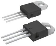 |

표면 실장 전자 부품

- SOIC(소형 집적 회로): 이것은 직사각형 모양에 각 면에 핀이 일렬로 배열된 형태의 집적 회로 패키지입니다.
- QFP(쿼드 플랫 패키지): 이러한 형태의 풋프린트는 부품 본체의 각 측면에서 직사각형 패턴으로 뻗어 나온 4줄의 리드로 구성됩니다.
- PLCC(플라스틱 리드 칩 캐리어): 이러한 형태의 풋프린트는 부품 본체 측면에서 직사각형 패턴으로 뻗어 나온 두 줄의 리드로 구성됩니다.
- PGA(핀 그리드 어레이): 이러한 형태의 풋프린트는 부품 본체 아래쪽에 핀 그리드가 배열된 형태입니다. 이후에 설명할 BGA와는 달리 소켓을 사용하여 장착해야 하므로 표면 실장 부품이라고 할 수는 없습니다.
- QFN(쿼드 플랫 무연): 이러한 형태의 풋프린트는 전자 부품 본체의 측면에서 직사각형 패턴으로 뻗어 나오는 4줄의 리드로 구성되지만, 부품 본체의 바닥에서는 리드가 뻗어 나오지 않습니다.
PLCC(플라스틱 리드 칩 캐리어): 이것은 정사각형 모양에 각 변에 핀이 일렬로 배열된 형태의 집적 회로 패키지입니다.
BGA (Ball Grid Array): 이러한 유형의 풋프린트는 부품 본체 아래쪽에 솔더 볼 격자로 구성됩니다.
SOT (작은 윤곽선) 트랜지스터): 이것은 직사각형 모양에 각 면에 핀이 일렬로 배열된 트랜지스터 패키지의 한 종류입니다.
표준화된 표면 실장형 폼팩터 크기

가장 많이 사용되는 몇 가지 예는 다음과 같습니다.
| 발자국 이름 | 표면 실장형 표준 크기 | 일반적인 적용 사례 |
| 201 | 0.6mm x 0.3mm | 이것들은 저항이나 콘덴서와 같은 소형 수동 부품에 사용됩니다. 크기가 작기 때문에 자동 픽앤플레이스 조립만 가능합니다. |
| 402 | 0.6mm x 0.4mm | |
| 603 | 0.6mm x 0.5mm | |
| 805 | 0.8mm x 0.5mm | |
| 1206 | 1.2mm x 0.6mm | |
| 오늘-23 | 2.9mm x 1.3mm | 이러한 소자는 일반적으로 트랜지스터 및 다이오드와 같은 대형 능동 부품에 사용됩니다. |
| 오늘-223 | 4.9mm x 3.1mm | |
| 오늘-89 | 6.1mm x 3.1mm | |
| 오늘-553 | 7.9mm x 5.3mm |
전자 부품 및 그 응용 분야에 대한 자세한 내용은 위키피디아에서 확인하세요. 전자 포털 또는 ~에서 전기전자공학회 (IEEE).
보충 자료 및 기법
- 회로 설계 기초: 회로도 및 배치 설계에 대한 이해.
- 인쇄회로기판(PCB) 제조: PCB 생산에 사용되는 기술 및 공정.
- 납땜 기술: 전자 부품을 효과적으로 납땜하는 방법.
- 마이크로컨트롤러 프로그램 작성: 아두이노나 라즈베리 파이 같은 마이크로컨트롤러 프로그래밍 입문.
- 아날로그 및 디지털 신호: 아날로그 신호와 디지털 신호의 차이점 및 응용 분야.
- 임베디드 시스템 개발: 임베디드 시스템용 하드웨어 및 소프트웨어 개발의 기초.
- 신호 처리: 전자 신호를 처리하고 분석하는 기술.
- 전자 장비 테스트 및 문제 해결: tools and methods for diagnosing 전자 회로 문제들.
- 전자파 적합성(EMC): 전자 부품 및 시스템이 EMC 표준을 준수하는지 이해하고 확인합니다.
전자 부품 관련 외부 링크
국제 표준
(링크 위에 마우스를 올려놓으면 콘텐츠에 대한 설명을 볼 수 있습니다.)
사용된 용어집
Automated Optical Inspection (AOI): 인쇄회로기판 및 기타 전자 조립품의 결함을 감지하기 위해 영상 기술을 사용하는 공정으로, 미리 정의된 기준에 따라 시각적 데이터를 분석하여 품질 관리 및 사양 준수를 보장합니다.
Bill Of Material (BOM): 제품 제조에 필요한 구성 요소, 하위 조립품 및 원자재를 수량 및 사양을 포함하여 자세히 나열한 구조화된 목록으로, 생산 계획 및 재고 관리에 사용됩니다.
Bill of Materials (BOM): 제품 제조에 필요한 구성 요소, 재료 및 수량을 자세히 나열한 종합 목록으로, 제조 및 엔지니어링 분야에서 생산 계획, 재고 관리 및 비용 추정을 용이하게 하기 위해 자주 사용됩니다.
Electromagnetic Compatibility (EMC): 전기 장치가 외부 전자기장의 간섭 없이 작동하고, 다른 장치에 간섭을 일으키는 수준의 전자기 에너지를 방출하지 않는 능력.
Institute of Electrical and Electronics Engineers (IEEE): 전기공학, 전자공학, 컴퓨터 과학 및 관련 분야의 기술 발전을 위해 출판물, 학술대회 및 표준 개발을 통해 헌신하는 전문 협회입니다. 전 세계 전문가와 연구자 간의 혁신과 협력을 촉진합니다.
Printed Circuit Board (PCB): 절연 재질로 만들어진 평평한 기판으로, 전도성 경로를 통해 전자 부품을 지지하고 연결합니다. 일반적으로 구리 시트를 에칭하여 제작됩니다. 회로 조립의 기초가 되며 부품 간의 전기적 연결을 용이하게 합니다.
Programmable Logic Controller (PLC): 산업 공정 자동화에 사용되는 디지털 컴퓨터로, 명령어를 저장하는 프로그래밍 가능한 메모리, 기계를 모니터링하고 제어하기 위한 입출력 인터페이스, 그리고 제어 알고리즘을 실행하는 프로세서로 구성됩니다.
Surface-Mount Technology (SMT): 인쇄회로기판 표면에 전자 부품을 직접 조립하는 방식으로, 소자의 밀도를 높이고 크기를 줄일 수 있습니다. 솔더 페이스트와 리플로우 솔더링 기술을 사용하여 부품을 접착합니다. 고속 완전 자동화 기계 조립에 최적화되어 있지만, 수동 조립도 가능합니다.