Product Design, Manufacturing & Innovation Resources
집 » 분자 전자공학

분자 전자공학

1974-11-15
  • Ari Aviram
  • Mark Ratner
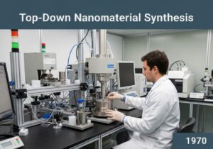
실험실 환경에서 분자 전선 및 스위치를 포함한 분자 전자 부품.

(설명을 위한 생성된 이미지입니다)

분자 전자공학은 개별 분자 또는 나노 크기의 분자 집합체를 기본적인 전자 부품으로 활용하는 분야입니다. 이 접근법은 기존의 실리콘 기반 기술을 훨씬 뛰어넘는 초소형 회로 구축을 목표로 합니다. 주요 구성 요소로는 분자 와이어, 스위치, 정류기 등이 있으며, 분자 궤도를 통한 전자 터널링과 같은 양자 역학적 특성을 이용하여 기능을 구현합니다.

The concept of molecular electronics, first conceptualized by Ari Aviram and Mark Ratner in 1974, represents a paradigm shift from top-down lithography to bottom-up self-assembly for creating electronic circuits. Their seminal paper proposed a molecular rectifier, a D-σ-A molecule (Donor-sigma bridge-Acceptor), which would allow current to flow preferentially in one direction, analogous to a semiconductor p-n diode. The principle relies on the alignment of molecular energy levels (HOMO and LUMO) under an applied bias voltage. When a voltage is applied, electrons can tunnel from an electrode, through the molecule’s orbitals, to the other electrode. The asymmetry in the D-A structure creates an asymmetric current-voltage (I-V) characteristic, which is the basis of rectification.

단순한 정류기를 넘어, 연구자들은 분자 와이어(예: 공액 고분자), 빛, 열 또는 전기장을 이용하여 '켜짐'과 '꺼짐' 상태를 전환할 수 있는 스위치, 심지어 분자 트랜지스터까지 구현해냈습니다. 주요 과제는 이러한 미세한 분자들을 거시적인 전극에 안정적으로 연결하고 안정적이고 재현 가능한 장치를 만드는 것입니다. 주사 터널링 현미경(STM) 브레이크 접합 및 기계적으로 제어 가능한 브레이크 접합(MCBJ)과 같은 기술은 실험실 환경에서 단일 분자의 전도도를 측정하는 데 사용됩니다. 완전한 규모의 분자 컴퓨터는 아직 먼 미래의 목표이지만, 그 원리는 분자의 전자적 특성이 특정 표적 분석물질에 결합할 때 변화하는 분자 센싱 분야나 유기 분자막을 통한 전하 이동에 의존하는 유기 발광 다이오드(OLED)와 같은 분야에 적용되고 있습니다.

이 분야는 양자 화학, 재료 과학 등을 융합하는 매우 학제적인 분야입니다. condensed matter physics. It promises not only extreme miniaturization but also novel functionalities derived from the unique quantum properties of individual molecules, potentially leading to devices with lower power consumption and entirely new computational models.

UNESCO Nomenclature: 2205
전자제품

유형

추상 시스템

분열

기초적인

용법

신흥 기술

전구체

  • 전자의 발견
  • 양자역학의 발전
  • 복잡한 유기 분자의 합성
  • 반도체 다이오드의 발명
  • 주사 터널링 현미경(STM)의 개발

응용 프로그램

  • 분자 규모 센서
  • 초고밀도 데이터 저장
  • 유기 발광 다이오드(OLED)
  • 분자 컴퓨팅 아키텍처의 잠재력

특허:

NA

잠재적 혁신 아이디어

  • biocompatible logic gates for in-vivo computing
  • self-assembling neural networks for pattern recognition
  • molecular sensors integrated into textiles for real-time health monitoring
  • catalytic surfaces with embedded electronic feedback loops
  • quantum dot-molecule hybrid systems for advanced photovoltaics
  • programmable matter where molecular switches alter material properties
  • ultra-low power memory based on molecular conformational changes
  • chemically-powered molecular motors for nanoscale robotics
Related to: molecular electronics, single-molecule, aviram-ratner, molecular rectifier, quantum tunneling, bottom-up fabrication, molecular switch, nanoelectronics.

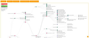
역사적 맥락

분자 전자공학

1965
1970
1970
1974-11-15
1980
1980
1980
1964
1968
1970
1970
1975
1980
1980
1980

(날짜를 알 수 없거나 관련이 없는 경우, 예를 들어 "유체역학"의 경우, 주목할 만한 등장 시기를 대략적으로 추정하여 제공합니다.)
10년차 기념일

고화질 이미지 및 다운로드는 등록된 회원에게만 100% 무료로 제공됩니다.

> 로그인 <