Micromecanizado de superficies para MEMS
1980
- Richard S. Muller
- Roger T. Howe
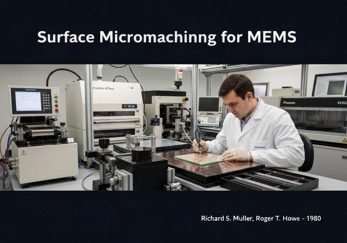
Fabricación mediante micromecanizado de superficies MEMS Los dispositivos se fabrican mediante la deposición y el modelado de películas delgadas sobre un sustrato. El proceso consiste en depositar una capa de sacrificio (como dióxido de silicio), modelarla, depositar una capa estructural (como polisilicio) y, finalmente, retirar la capa de sacrificio para liberar la estructura mecánica. Este proceso permite crear microestructuras complejas e independientes directamente sobre la superficie de la oblea.
Surface micromachining is a cornerstone of MEMS fabrication, enabling the creation of intricate mechanical systems on top of a substrate, typically a silicon wafer. The process is additive, building structures layer by layer, which contrasts with the subtractive nature of bulk micromachining. A typical process flow begins with the deposition of an isolation layer, like silicon nitride, on the substrate. Following this, a sacrificial layer, often a type of silicon dioxide called phosphosilicate glass (PSG), is deposited using Low-Pressure Chemical Vapor Deposition (LPCVD). This layer is then patterned using photolithography and etching, defining the areas where the final structure will be anchored to the substrate and the gaps beneath moving parts.
A continuación, se deposita la capa estructural, generalmente silicio policristalino (polisilicio), sobre la capa de sacrificio con el patrón definido. Esta capa de polisilicio se modela posteriormente para definir la geometría de los componentes mecánicos deseados, como vigas, engranajes o membranas. Esta secuencia de deposición y modelado de las capas de sacrificio y estructurales puede repetirse varias veces para crear estructuras multinivel de gran complejidad. El paso final y crucial es el proceso de «liberación». La oblea se sumerge en un agente de grabado químico, normalmente ácido fluorhídrico (HF), que elimina selectivamente las capas de PSG de sacrificio sin dañar las capas estructurales de polisilicio ni la capa de aislamiento de nitruro de silicio. Esto permite que las estructuras de polisilicio se muevan libremente, suspendidas sobre el sustrato mediante sus anclajes designados.
Una ventaja importante de esta técnica es su compatibilidad inherente con los procesos estándar de fabricación de circuitos integrados CMOS. Esto permite la integración monolítica de dispositivos MEMS con su electrónica de control y procesamiento de señales en el mismo chip, lo que da como resultado sistemas más pequeños, económicos y de mayor rendimiento. Sin embargo, el micromecanizado de superficies no está exento de desafíos. El principal modo de fallo durante la liberación es la "adherencia", donde las estructuras liberadas, una vez húmedas, son atraídas hacia el sustrato por fuerzas capilares durante el secado y quedan permanentemente adheridas debido a fuerzas intermoleculares como la atracción de van der Waals. Se han desarrollado diversas estrategias antiadherentes, como el secado con CO2 supercrítico o recubrimientos superficiales especiales, para mitigar este problema crítico.
UNESCO Nomenclature: 3313
- Ingeniería industrial
Precursores
- photolithography techniques from the semiconductor industry
- chemical vapor deposition (CVD) for thin film growth
- wet and dry etching processes
- integrated circuit (IC) fabrication technology
Aplicaciones
- digital micromirror devices (DMDs) in projectors
- inertial sensors (accelerometers and gyroscopes) in smartphones
- pressure sensors
- inkjet printer heads
- RF MEMS switches
Ideas para posibles innovaciones
Debido al bloqueo del tráfico generado por bots, que actualmente supera los 40.000 al día, este contenido está reservado para los miembros de la comunidad.
> Iniciar sesión < o > Registrarse < (100% gratis) para acceder a esto, al igual que a todo el demás contenido y herramientas restringidos.
Relacionado con: micromecanizado de superficies, MEMS, fabricación, película delgada, polisilicio, capa de sacrificio, grabado, microfabricación, litografía, adherencia.