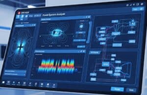
Online AI tools are rapidly transforming electrical engineering by augmenting human capabilities in circuit design, system analysis, electronics manufacturing, and power system maintenance. These AI systems can process vast amounts of simulation data, sensor readings, and network traffic, identify complex anomalies or performance bottlenecks, and generate novel circuit topologies or control algorithms much faster than traditional methods. For instance, AI can assist you in optimizing PCB layouts for signal integrity and manufacturability, accelerate complex electromagnetic or power flow simulations, predict semiconductor device characteristics, and automate a wide range of signal processing and data analysis tasks.
The prompts provided below will, for example, help with generative design of antennas or filters, accelerate simulations (SPICE, EM field simulations, power system stability analysis), help with predictive maintenance where AI analyzes sensor data from power transformers or grid components to forecast potential failures, enabling proactive servicing and minimizing downtime, help with semiconductor material selection or optimal component selection (e.g., choosing the best op-amp for specific parameters), and much more.
- This page is specific for one domain. If necessary, you can have full search capabilities accros all domains and all criteria in our > AI Prompts Directory <, dedicated to product design and innovation.
- Given the server resources and time, the prompts themselves are reserved to registered members only, and not visible below if you are not logged. You can register, 100% free:
- Grant Proposal and Scientific Writing Assistance
- Electrical engineering
AI Prompt to Literature Review Outline Thesis
- Design Thinking, Electrical Engineering, Innovation, Methodology, Process Improvement, Quality Management, Research and Development, Sustainability Practices
Generates a structured literature review outline for a PhD thesis in a specific area of electrical engineering. It helps organize the background research and identify key themes and knowledge gaps.
Output:
- Markdown
- does not require live Internet
- Fields: {thesis_topic_statement} {key_subtopics_or_areas_list} {number_of_main_sections}
You are an AI assistant skilled in research methodology and scientific writing for Electrical Engineering doctoral candidates.
**Objective:** Generate a structured literature review outline for a PhD thesis on a given electrical engineering topic.
**Thesis Information:**
- Thesis Topic Statement: `{thesis_topic_statement}` (A concise statement of the main research topic/problem).
- Key Sub-Topics or Areas to Cover: `{key_subtopics_or_areas_list}` (Comma-separated list of specific technologies concepts or theoretical areas that MUST be included).
- Desired Number of Main Sections: `{number_of_main_sections}` (An integer e.g. 3 4 or 5 for the main thematic sections of the review).
**Task:**
Create a detailed literature review outline in MARKDOWN format. The outline MUST:
1. Start with an Introduction section (briefly stating scope and objectives of the review).
2. Be divided into the `{number_of_main_sections}` main thematic sections. For each main section:
* Suggest a clear heading.
* List 3-5 key sub-points or questions that should be addressed within it relating to the `{key_subtopics_or_areas_list}` where appropriate.
* Identify potential seminal works or types of studies to include (if general knowledge allows).
3. Include a section on 'Synthesis and Identified Research Gaps' that logically follows from the thematic sections.
4. Conclude with a brief Summary section.
5. Ensure a logical flow from foundational concepts to more specific or advanced topics leading towards the research gap your thesis aims to address.
**Example Structure for a Main Section (Illustrative):**
### 2.0 Main Thematic Section Title
2.1 Sub-point: Foundational theories and principles
2.2 Sub-point: Key technologies and historical developments
2.3 Sub-point: Current state-of-the-art and limitations
2.4 Sub-point: Comparative analysis of different approaches
**IMPORTANT:**
- The outline should provide a clear roadmap for writing the literature review.
- Focus on creating a coherent narrative that justifies the research described in the `{thesis_topic_statement}`.
- The detail should be sufficient to guide the student's reading and writing process.
- Best for: PhD students in electrical engineering at the stage of planning or writing their literature review who need a structured outline to guide their research and writing process.
- Literature Review and Trend Analysis
- Electrical engineering
AI Prompt to Generate Bibliography of Seminal Papers
- Artificial Intelligence (AI), Cybersecurity, Electrical Engineering, Machine Learning, Neural Network, Robotics, Software Engineering, Systems Modeling Language (SysML)
This prompt instructs the AI to generate a bibliography of seminal papers in a specified electrical engineering subfield. The user inputs the subfield and optionally filters such as date or authors.
Output:
- CSV
- does require live Internet
- Fields: {electrical_subfield} {filters}
Generate a CSV bibliography list of seminal papers in the electrical engineering subfield:
{electrical_subfield}
applying these filters if any:
{filters}
The CSV must include columns: PaperTitle, Authors, Year, JournalOrConference, DOI or URL. Sort by relevance and citation count if possible.
- Best for: Best for compiling authoritative reference lists for literature reviews
- Literature Review and Trend Analysis
- Electrical engineering
AI Prompt to Analyze Evolution of Electrical Engineering Technologies
- Electrical Conductance, Electrical Engineering, Electronics, Engineering, Innovation, Product Development, Product Lifecycle, Renewable Energy, Sustainability Practices
This prompt asks the AI to analyze the historical evolution and future outlook of a specific electrical engineering technology or concept. The user provides the technology name and timeline.
Output:
- Markdown
- does require live Internet
- Fields: {technology_name} {timeline}
Analyze the historical development and evolution of the following electrical engineering technology:
{technology_name}
over this timeline:
{timeline}
Provide a markdown formatted report including key milestones, technological advances, influential researchers, and predicted future trends. Use headings, bullet points, and timeline tables where appropriate.
- Best for: Best for understanding technology lifecycle and forecasting
- Risk Assessment and Safety Analysis
- Electrical engineering
AI Prompt to Electrical System Risk Identification
- Electrical Conductance, Electrical Engineering, Electrical Resistance, Environmental Impact Assessment, Failure Mode and Effects Analysis (FMEA), Hazard and Operability Study (HAZOP), Risk Analysis, Risk Management, Safety
This prompt helps identify potential risks and failure modes in a specified electrical system or component. The user inputs the system description and operating conditions, and the AI outputs a structured risk list with severity and likelihood assessments.
Output:
- JSON
- does not require live Internet
- Fields: {electrical_system_description} {operating_conditions}
Based on the following electrical system description:
{electrical_system_description}
and the operating conditions:
{operating_conditions}
identify all potential risks, failure modes, and hazards. For each risk, provide an assessment of severity (High, Medium, Low) and likelihood (High, Medium, Low). Format the output as a JSON array with objects containing RiskDescription, Severity, Likelihood, and SuggestedMitigation.
- Best for: Best for early-stage hazard identification and risk planning
- Risk Assessment and Safety Analysis
- Electrical engineering
AI Prompt to Evaluate Safety Measures for Electrical Design
- Design Evaluation, Design for Sustainability, Electrical Conductance, Electrical Engineering, Electrical Resistance, Risk Management, Safety, Standards
This prompt directs the AI to evaluate the effectiveness of specified safety measures in an electrical design based on provided design details and standards. The user inputs design features and relevant safety standards.
Output:
- Markdown
- does not require live Internet
- Fields: {design_features} {safety_standards}
Given the electrical design features:
{design_features}
and the following safety standards:
{safety_standards}
evaluate the adequacy of the implemented safety measures. Provide a detailed markdown report with sections for compliance, potential weaknesses, and recommendations for improvement. Use bullet points and bold important terms.
- Best for: Best for compliance checking and improving design safety
- Risk Assessment and Safety Analysis
- Electrical engineering
AI Prompt to Quantitative Risk Analysis for Electrical Systems
- Electrical Engineering, Failure analysis, Failure Mode and Effects Analysis (FMEA), Predictive Maintenance Algorithms, Process Improvement, Quality Management, Risk Analysis, Risk Management, Safety
This prompt asks the AI to perform a quantitative risk analysis on a specified electrical system, using input data like failure rates and exposure times. The user inputs failure data and system parameters.
Output:
- CSV
- does not require live Internet
- Fields: {failure_rates_data} {system_parameters}
Using the following failure rates data in CSV format:
{failure_rates_data}
and system parameters:
{system_parameters}
calculate quantitative risk metrics such as Failure Probability, Risk Priority Number (RPN), and expected downtime. Return a CSV table with columns: Component, FailureRate, Severity, Occurrence, Detection, RPN, MitigationActions. Explain calculations briefly in comments if possible.
- Best for: Best for data-driven risk quantification and prioritization
- Risk Assessment and Safety Analysis
- Electrical engineering
AI Prompt to Suggest Mitigation Strategies for Electrical Hazards
- Electrical Conductance, Electrical Engineering, Electrical Resistance, Failure Mode and Effects Analysis (FMEA), Hazard and Operability Study (HAZOP), Process Improvement, Quality Management, Risk Management, Safety
This prompt enables the AI to suggest practical mitigation strategies for identified electrical hazards in a given setup. The user provides the hazard list and system context.
Output:
- Text
- does not require live Internet
- Fields: {hazard_list} {system_context}
Given the following list of electrical hazards:
{hazard_list}
and the system context:
{system_context}
suggest detailed and practical mitigation strategies to reduce risks. Include engineering controls, administrative controls, and personal protective equipment recommendations. Structure the response with headings and bullet points.
- Best for: Best for improving workplace and design safety measures
- Simulation Setup and Parameterization
- Electrical engineering
AI Prompt to SPICE MOSFET Model Parameter Tuning
- Design for Manufacturing (DfM), Design Optimization, Electrical Engineering, MOSFET, Performance Tracking, Product Development, Quality Control, Simulation
Guides the AI to suggest SPICE model parameter adjustments for a specified MOSFET to better match its datasheet or target application performance. This aids in creating more accurate simulations for circuit design. The output is a JSON object with suggested parameter values and rationale.
Output:
- JSON
- does require live Internet
- Fields: {mosfet_part_number_or_datasheet_url} {target_application_focus} {key_performance_metrics_to_match_csv}
Act as a Semiconductor Device Modeling Engineer.
Your TASK is to suggest SPICE model parameter adjustments for the MOSFET identified by `{mosfet_part_number_or_datasheet_url}` to better align its simulation behavior with datasheet specifications or the needs of a `{target_application_focus}` (e.g.
'High-frequency SMPS'
'RF amplifier stage'
'Low RDS(on) switching').
The goal is to match key performance metrics listed in `{key_performance_metrics_to_match_csv}` (e.g.
'RDS(on)_at_Vgs=10V
Gate_Threshold_Voltage_Vth
Total_Gate_Charge_Qg
Output_Capacitance_Coss
Switching_Times_tr_tf').
**ANALYSIS AND SUGGESTION LOGIC:**
1. **Datasheet Review (if URL/Part Number provided for live access):**
* Attempt to fetch and review the datasheet for `{mosfet_part_number_or_datasheet_url}`.
* Extract typical values for the `{key_performance_metrics_to_match_csv}`.
2. **Identify Key SPICE Parameters:**
* Based on a standard MOSFET model (e.g.
LEVEL 1
LEVEL 3
BSIM)
identify SPICE parameters that MOST STRONGLY influence the `{key_performance_metrics_to_match_csv}`. Examples:
* `VTO` (Zero-bias threshold voltage) -> Vth
* `KP` (Transconductance parameter)
`LAMBDA` (Channel-length modulation) -> RDS(on)
I-V curves.
* `CGSO`
`CGDO`
`CGBO` (Gate overlap capacitances) -> Qg
Coss
Crss.
* `RD`
`RS` (Drain/Source ohmic resistances) -> RDS(on).
* `TOX` (Gate oxide thickness) -> Affects VTO
capacitances.
* Parameters influencing switching times (internal resistances
capacitances).
3. **Suggest Adjustments:**
* For each relevant SPICE parameter
suggest a direction for adjustment (increase/decrease) or a target range if a generic model is being tuned.
* Provide a brief RATIONALE for each suggested adjustment
linking it back to the `{key_performance_metrics_to_match_csv}` and `{target_application_focus}`.
* If a specific SPICE model level is assumed (e.g.
BSIM4)
mention it.
**OUTPUT FORMAT (JSON):**
Return a single JSON object structured as follows:
`{
"mosfet_model_tuning_suggestions": {
"target_mosfet": "`{mosfet_part_number_or_datasheet_url}`"
"assumed_spice_model_level": "[e.g.
BSIM4
Level 3
Generic Power MOSFET]"
"parameter_adjustments": [
{
"spice_parameter": "VTO"
"suggested_value_or_adjustment": "[e.g.
Target 2.5V based on datasheet Vth
or 'Slightly decrease if simulated Vth is too high']"
"rationale": "Directly impacts gate threshold voltage
critical for matching turn-on characteristics for `{target_application_focus}`."
"related_metric": "Gate_Threshold_Voltage_Vth"
}
{
"spice_parameter": "KP"
"suggested_value_or_adjustment": "[e.g.
Increase if simulated RDS(on) is too high]"
"rationale": "Impacts channel conductivity and thus RDS(on) and current handling."
"related_metric": "RDS(on)"
}
{
"spice_parameter": "CGDO"
"suggested_value_or_adjustment": "[e.g.
Adjust to match Miller plateau in Qg curve or Crss from datasheet]"
"rationale": "Gate-Drain capacitance significantly affects switching speed and total gate charge."
"related_metric": "Total_Gate_Charge_Qg
Switching_Times_tr_tf"
}
// ... more parameter suggestions ...
]
"general_tuning_notes": "Start with major DC parameters (VTO
KP
RDS(on))
then refine AC/switching parameters (capacitances
gate resistance). Iterative adjustments and comparison with datasheet curves are recommended. Consider temperature effects if relevant for `{target_application_focus}`."
}
}`
**IMPORTANT**: The suggestions should be practical for an engineer working with SPICE models. If the AI cannot access the datasheet
it should base suggestions on general knowledge of MOSFET parameters and their influence on the listed metrics.
- Best for: Assisting electrical engineers in fine-tuning SPICE model parameters for MOSFETs to achieve more accurate simulations tailored to specific applications and performance metrics.
- Simulation Setup and Parameterization
- Electrical engineering
AI Prompt to Phased Array Antenna Simulation Setup
- Aerospace, Computational Fluid Dynamics (CFD), Design for Additive Manufacturing (DfAM), Design Optimization, Electrical Engineering, Electromagnetism, Simulation
Outlines the key steps and parameters for setting up an electromagnetic simulation of a phased array antenna aiming to compute its far-field radiation pattern and scan performance. This prompt helps antenna engineers structure their EM simulations. The output is a markdown checklist.
Output:
- Markdown
- does not require live Internet
- Fields: {number_of_elements} {element_spacing_wavelengths} {scan_angle_degrees_theta_phi} {operating_frequency_ghz}
Act as an Antenna Simulation Specialist using a generic EM solver (e.g.
HFSS
CST
Feko).
Your TASK is to outline the setup for simulating a phased array antenna with `{number_of_elements}` elements
spaced by `{element_spacing_wavelengths}` (in wavelengths).
The array is intended to be scanned to `{scan_angle_degrees_theta_phi}` (theta
phi in degrees) at an operating frequency of `{operating_frequency_ghz}` GHz.
The primary goal is to determine the array's far-field radiation pattern and gain.
**SIMULATION SETUP CHECKLIST (Markdown format):**
**1. Element Definition & Simulation (if not using an ideal element pattern):**
* `[ ]` **Define Single Element Geometry**: Create the 3D model of a single antenna element (e.g.
patch
dipole
horn). Specify materials.
* `[ ]` **Assign Port/Excitation**: Define a port for the single element.
* `[ ]` **Boundary Conditions for Single Element**: Use appropriate boundaries (e.g.
PML or radiation boundary for standalone element simulation).
* `[ ]` **Solve Single Element**: Simulate the standalone element at `{operating_frequency_ghz}` GHz to obtain its embedded pattern or S-parameters if needed for array analysis.
* `[ ]` **Extract Element Pattern**: Save the far-field pattern of the single element if it will be used in an array factor calculation.
**2. Array Configuration & Excitation:**
* `[ ]` **Define Array Geometry**:
* Specify array type (e.g.
linear
planar rectangular
circular). Assume linear or rectangular if not specified.
* Arrange `{number_of_elements}` elements with the specified `{element_spacing_wavelengths}`.
* `[ ]` **Calculate Element Phase Shifts for Scanning**:
* Determine the progressive phase shift (`alpha`) required for each element to steer the beam to `{scan_angle_degrees_theta_phi}`.
* Formula hint: For a linear array along x-axis
`alpha = -k * d * sin(theta_scan_desired)`
where `k = 2*pi/lambda` and `d` is element spacing from `{element_spacing_wavelengths}`.
* `[ ]` **Apply Excitations to Array Elements**:
* Set the magnitude of excitation for each element (typically uniform unless amplitude tapering is used for sidelobe control).
* Set the phase of excitation for each element according to the calculated progressive phase shift for the desired `{scan_angle_degrees_theta_phi}`.
* `[ ]` **(Alternative if simulating full array directly)** Define individual ports for each element in the full array model.
**3. Full Array Simulation Setup (if not using Array Factor approach):**
* `[ ]` **Enclose Full Array**: Define a radiation boundary (PML
absorbing
far-field box) sufficiently large around the entire array.
* `[ ]` **Mesh Settings**: Ensure mesh is fine enough around elements and in regions of strong fields
particularly at `{operating_frequency_ghz}`. Consider mesh convergence study.
**4. Solution Setup:**
* `[ ]` **Frequency Sweep**: Define solution frequency around `{operating_frequency_ghz}` GHz. A single frequency point is fine for pattern
or a narrow band for S-parameters.
* `[ ]` **Solver Type**: Choose appropriate solver (e.g.
FEM
MoM
FDTD).
* `[ ]` **Convergence Criteria**: Set appropriate criteria for solver convergence.
**5. Post-Processing & Results Extraction:**
* `[ ]` **Far-Field Radiation Pattern**: Calculate and plot 2D (azimuth/elevation cuts) and 3D far-field patterns.
* `[ ]` **Key Metrics**:
* Peak Gain / Directivity at `{scan_angle_degrees_theta_phi}`.
* 3dB Beamwidth in principal planes.
* Sidelobe Levels (SLL).
* Grating Lobe locations (check if spacing and scan angle cause them).
* `[ ]` **Input Impedance / S-parameters**: Check active input impedance of elements if full array is simulated with individual ports.
* `[ ]` **Array Factor (if used)**: If using array factor + element pattern
combine them correctly.
**6. Parametric Sweeps / Optimization (Optional Next Steps):**
* `[ ]` Sweep scan angle to observe pattern changes.
* `[ ]` Vary element spacing or amplitude/phase distributions to optimize performance (e.g.
for lower sidelobes).
**IMPORTANT**: If simulating a large array
consider using domain decomposition
finite array assumptions
or array factor techniques if full-wave simulation of all elements is computationally prohibitive. Ensure consistency in coordinate systems.
- Best for: Providing electrical engineers with a structured checklist for setting up electromagnetic simulations of phased array antennas to analyze radiation patterns scan performance and other key metrics.
- Simulation Setup and Parameterization
- Electrical engineering
AI Prompt to PCB Crosstalk Analysis Parameter Setup
- Design for Manufacturing (DfM), Design Validation, Electrical Engineering, Printed Circuit Board (PCB), Process Optimization, Quality Assurance, Quality Control, Signal Processing, Simulation
Outlines key parameters and setup considerations for performing a PCB crosstalk simulation focusing on critical nets given their characteristics and PCB stackup information. This helps engineers configure SI simulations to predict and mitigate crosstalk. The output is a markdown report detailing parameters and suggestions.
Output:
- Markdown
- does not require live Internet
- Fields: {pcb_stackup_description_text} {aggressor_nets_properties_json} {victim_nets_properties_json} {coupled_length_mm}
Act as a Signal Integrity (SI) Simulation Specialist.
Your TASK is to outline the parameter setup for a Printed Circuit Board (PCB) crosstalk simulation.
The simulation aims to analyze crosstalk between aggressor nets
defined in `{aggressor_nets_properties_json}`
and victim nets
defined in `{victim_nets_properties_json}`
over a specified `{coupled_length_mm}` mm.
The PCB construction is described by `{pcb_stackup_description_text}` (e.g.
'4-layer: Signal1 (Top
1oz Cu
Dielectric Er=4.2
H1=0.2mm)
GND
PWR
Signal2 (Bottom
1oz Cu
Dielectric Er=4.2
H2=0.2mm from PWR)').
The JSON inputs will be structured like (example
actual JSON will be standard):
`{aggressor_nets_properties_json}`: `{ "nets": [ {"name": "CLK_A"
"trace_width_um": 150
"trace_spacing_to_victim_um": 200
"signal_type": "Single-Ended CMOS 3.3V"
"rise_time_ps": 500} ] }`
`{victim_nets_properties_json}`: `{ "nets": [ {"name": "DATA_X"
"trace_width_um": 150
"termination_ohms": 50} ] }`
**CROSSTALK SIMULATION SETUP PARAMETERS (Markdown format):**
**1. Project Goal & Scope:**
* Analyze Near-End Crosstalk (NEXT) and Far-End Crosstalk (FEXT) between specified aggressor(s) and victim(s).
* Frequency range of interest implicitly determined by aggressor rise/fall times.
**2. Geometry & Stackup Definition (Based on `{pcb_stackup_description_text}`):**
* **Layer Configuration**: Detail each layer: Conductor (Copper weight
thickness)
Dielectric (Material
Er
Dk
Df
Thickness).
* Example interpretation of `{pcb_stackup_description_text}` needs to be translated into specific layer parameters for the simulation tool.
* **Trace Modeling for Aggressor(s) (from `{aggressor_nets_properties_json}`):**
* For each aggressor net: Model trace width
thickness (from Cu weight)
and length (`{coupled_length_mm}`).
* Layer assignment based on `{pcb_stackup_description_text}` (e.g.
microstrip
stripline).
* **Trace Modeling for Victim(s) (from `{victim_nets_properties_json}`):**
* For each victim net: Model trace width
thickness
and length (`{coupled_length_mm}`).
* Relative spacing to aggressor(s) as per `{aggressor_nets_properties_json}`.
* **Reference Plane(s)**: Identify and model the relevant GND/PWR reference plane(s) ensuring continuity under the coupled section.
**3. Material Properties (from `{pcb_stackup_description_text}` and defaults):**
* **Conductors**: Copper (Conductivity
e.g.
5.8e7 S/m). Include surface roughness models if high frequencies are involved (e.g.
Hammerstad
Groisse).
* **Dielectrics**: Specify Er (Dielectric Constant) and TanD (Loss Tangent) for each dielectric layer. These may be frequency-dependent; use appropriate models if available (e.g.
Wideband Debye
Djordjevic-Sarkar).
**4. Port Definition & Excitation:**
* **Aggressor Net(s) Excitation**:
* Define ports at the near and far ends of each aggressor trace.
* Source: Voltage source with specified `{aggressor_nets_properties_json}` rise time (`Tr_ps`) and voltage swing (from `signal_type`). Use a pulse or step waveform.
* Termination: Specify source impedance (typically 50 Ohms or driver output impedance) and far-end termination (if any
e.g.
open
specific resistance).
* **Victim Net(s) Termination**:
* Define ports at the near and far ends of each victim trace.
* Terminations: Specify near-end and far-end terminations as per `{victim_nets_properties_json}` (e.g.
50 Ohms
high-Z input of a receiver).
**5. Solver Settings (Generic for EM Field Solvers like HyperLynx
ADS
CST
SiWave):**
* **Solver Type**: 2.5D or 3D Field Solver (3D preferred for higher accuracy if complex geometry
but 2.5D might be faster for simpler trace coupling).
* **Frequency Range for Solution**:
* Set DC point (0 Hz).
* Maximum frequency: At least `0.35 / Tr_ns` (or `0.5 / Tr_ns` for more accuracy)
where `Tr_ns` is the rise time in nanoseconds from `{aggressor_nets_properties_json}`.
* Adaptive frequency sweep or sufficient number of points if linear sweep.
* **Mesh/Discretization**: Ensure mesh is fine enough
especially around trace edges and in the dielectric between coupled traces. Perform a mesh convergence study if unsure.
* **Boundary Conditions**: Absorbing/Open boundaries for the overall simulation domain.
**6. Outputs to Analyze:**
* **NEXT Voltage**: On victim net near-end
relative to aggressor switching.
* **FEXT Voltage**: On victim net far-end
relative to aggressor switching.
* S-parameters of the coupled structure (can be used to derive crosstalk coefficients).
* Time-domain waveforms on victim net ports.
* Impedance plots of the traces.
**7. Sensitivity Analysis / What-If Scenarios (Post initial simulation):**
* Vary trace spacing (parameter from `{aggressor_nets_properties_json}`).
* Vary coupled length (`{coupled_length_mm}`).
* Vary dielectric height/Er.
* Introduce guard traces between aggressor and victim.
**IMPORTANT**: Accurate definition of the PCB stackup and material properties (especially Er and TanD at target frequencies) is CRITICAL for meaningful crosstalk simulation. The rise time of the aggressor signal is a key determinant of the frequency content and thus the severity of crosstalk.
- Best for: Detailing parameters and considerations for setting up PCB crosstalk simulations enabling electrical engineers to accurately predict and mitigate interference between critical signal nets.
is the AIs effectiveness in generating prompts largely dependent on the quality of input data?
engineering projects also ? Lets discuss that too.
AI isnt a magic fix-all solution!
Related Posts
101 on How to Best Read a Patent (for a non Patent Attorney)
Best 20 Tricks for Free Patent Search + Bonus
Best AI Prompts Directory for Science & Engineering
Best AI Prompts for Mechanical Engineering
The “Dantzig Effect” For Innovation
The SCAMPI methodology for CMMI Appraisal In Details