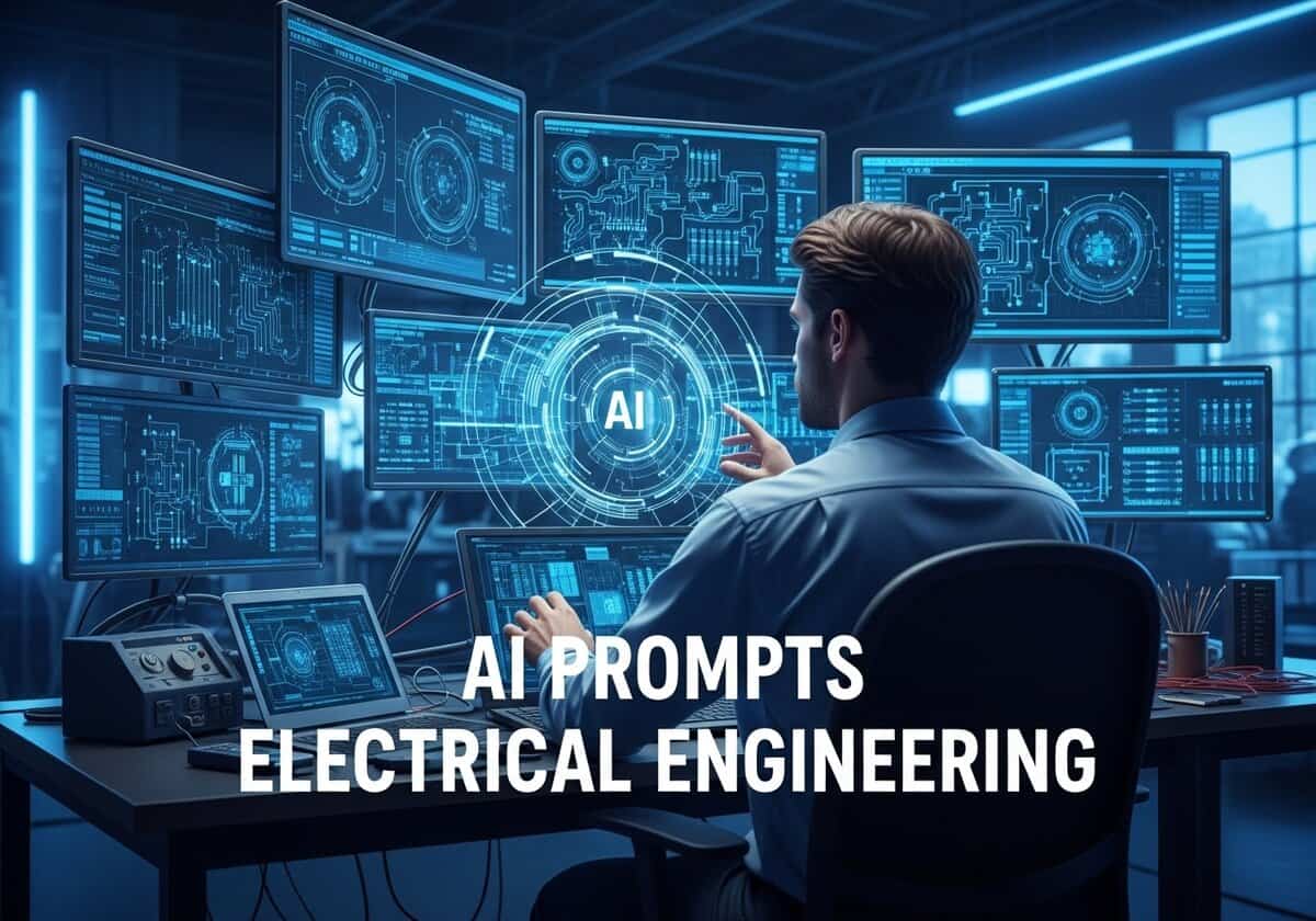
Online-KI-Tools verändern die Elektrotechnik rapide, indem sie die menschlichen Fähigkeiten bei der Schaltungsentwicklung, der Systemanalyse und der Elektronik ergänzen. Herstellungund die Wartung von Stromversorgungssystemen. Diese KI-Systeme können große Mengen an Simulationsdaten, Sensormesswerten und Netzwerkverkehr verarbeiten, komplexe Anomalien oder Leistungsengpässe erkennen und neuartige Schaltungstopologien oder Steuerungsalgorithmen viel schneller als herkömmliche Methoden entwickeln. KI kann Sie beispielsweise bei der Optimierung von PCB-Layouts im Hinblick auf Signalintegrität und Herstellbarkeit unterstützen, komplexe elektromagnetische oder Leistungsflusssimulationen beschleunigen, die Eigenschaften von Halbleiterbauelementen vorhersagen und eine Vielzahl von Aufgaben automatisieren. Signalverarbeitung und Datenanalyseaufgaben.
Die nachstehenden Aufforderungen helfen beispielsweise beim generativen Entwurf von Antennen oder Filtern, beschleunigen Simulationen (SPICE, EM-Feldsimulationen, Stabilitätsanalysen von Stromversorgungssystemen), helfen bei der vorausschauenden Wartung, bei der KI Sensordaten von Leistungstransformatoren oder Netzkomponenten analysiert, um potenzielle Ausfälle vorherzusagen, was eine proaktive Wartung ermöglicht und Ausfallzeiten minimiert, helfen bei der Auswahl von Halbleitermaterialien oder optimalen Komponenten (z. B. Auswahl des besten Operationsverstärkers für bestimmte Parameter) und vieles mehr.
- Diese Seite ist spezifisch für eine Domain. Bei Bedarf können Sie in unserer > Suchmaschine nach allen Domains und allen Kriterien suchen. AI Prompts Verzeichnis <, gewidmet dem Produktdesign Und Innovation.
- Angesichts der Server-Ressourcen und des Zeitaufwands sind die Eingabeaufforderungen selbst nur registrierten Mitgliedern vorbehalten und unten nicht sichtbar, wenn Sie nicht angemeldet sind. Sie können sich registrieren, 100% kostenlos:
Mitgliedschaft erforderlich
Sie müssen Mitglied sein, um auf diesen Inhalt zugreifen zu können.
- Risikobewertung und Sicherheitsanalyse
- Elektroingenieurwesen
AI Aufforderung an FMEA for Medical Electrical Equipment PSU
- Design für die Fertigung (DfM), Fehlermöglichkeits- und Einflussanalyse (FMEA), Gefahren- und Betriebsfähigkeitsstudie (HAZOP), Gesundheitspflege, Medizinische Geräte, Qualitätskontrolle, Qualitätsmanagement, Risikomanagement, Sicherheit
Generates a preliminary Failure Modes and Effects Analysis (FMEA) table for the power supply unit (PSU) of a specified medical electrical equipment focusing on patient and operator safety. This helps engineers proactively consider risks during PSU design or selection. The output is a CSV formatted FMEA table.
Ausgabe:
- CSV
- erfordert kein Live-Internet
- Fields: {medical_equipment_type} {psu_type_and_key_functions_text} {relevant_safety_standard_e_g_iec60601}
Act as a Medical Device Quality and Safety Engineer
specializing in electrical safety and FMEA.
Your TASK is to generate a preliminary Failure Modes and Effects Analysis (FMEA) table for the Power Supply Unit (PSU) of a `{medical_equipment_type}` (e.g.
'Portable Ultrasound Scanner'
'Vital Signs Monitor'
'Surgical Laser System').
The PSU is described by `{psu_type_and_key_functions_text}` (e.g.
'Internal AC/DC SMPS
provides isolated 12V
5V
and 24V outputs
mains input filtering'
'External medical grade AC adapter with DC output').
Consider requirements from `{relevant_safety_standard_e_g_iec60601}` (e.g.
IEC 60601-1 3rd Edition
focusing on Means of Protection - MOPP/MOOP).
**PRELIMINARY FMEA TABLE (Output as CSV String):**
**CSV Header**: `Item_Function
Potential_Failure_Mode
Potential_Effect_of_Failure_Local_PSU
Potential_Effect_of_Failure_System_Medical_Device
Potential_Effect_of_Failure_Patient_Operator
Potential_Cause_of_Failure
Current_Controls_Prevention_Detection
Severity_S_1_5
Occurrence_O_1_5
Detection_D_1_5
Risk_Priority_Number_RPN
Recommended_Actions_Further_Considerations`
**FMEA Logic to Populate Rows (AI to generate 3-5 example rows):**
For key functional blocks or components within a typical PSU as per `{psu_type_and_key_functions_text}` (e.g.
Mains Input Filter
Rectifier
PFC Stage
Isolation Transformer
Output Rectifier/Filter
Control Circuitry
Enclosure/Connectors):
1. **Item/Function**: The PSU sub-circuit or function.
2. **Potential Failure Mode**: How it could fail (e.g.
Short circuit
Open circuit
Component drift
Loss of isolation
Overvoltage output
No output).
3. **Potential Effect (Local
System
Patient/Operator)**: Consequences at different levels.
* Focus on safety implications related to `{relevant_safety_standard_e_g_iec60601}`: electric shock
burns
incorrect device operation affecting diagnosis/treatment.
4. **Potential Cause**: Why the failure mode might occur (e.g.
Component end-of-life
Overstress
Manufacturing defect
Environmental factors
Design flaw).
5. **Current Controls**: Typical design features or tests that prevent/detect the failure (e.g.
Fuses
MOVs
Proper insulation/creepage/clearance
Production testing
Component derating
Shielding).
6. **Severity (S)**: Impact on patient/operator safety (1=Low
5=Catastrophic). Consider `{relevant_safety_standard_e_g_iec60601}` context.
7. **Occurrence (O)**: Likelihood of the cause (1=Remote
5=Frequent).
8. **Detection (D)**: Likelihood of detecting failure mode/cause BEFORE harm occurs (1=High
5=Very Low/Impossible).
9. **RPN**: S * O * D.
10. **Recommended Actions**: Further design analysis
testing
or control improvements.
**Example CSV Rows (Conceptual - AI to generate specific content):**
`Mains_Input_Filter
Capacitor_Short_Y-cap_to_Earth
Loss_of_filtering
Increased_conducted_EMI
Potential_for_enclosure_to_become_live_if_PE_is_faulty
Electric_shock_to_operator_or_patient
Component_failure_due_to_overvoltage_or_defect
Safety_certified_Y-capacitors
Production_hipot_test
Proper_PE_connection
5
2
3
30
Verify_Y-cap_rating_and_PE_integrity
Consider_redundant_PE_path_if_risk_high`
`Isolation_Transformer
Primary-to-Secondary_Winding_Short
Loss_of_isolation
High_voltage_on_secondary_side
Entire_medical_device_secondary_circuitry_becomes_live
Severe_electric_shock_risk_to_patient_and_operator
Insulation_breakdown_due_to_age
overvoltage
or_manufacturing_defect
Reinforced_or_double_insulation_design_as_per_IEC60601-1
100%_hipot_testing_in_production
Use_of_certified_transformer
5
1
2
10
Ensure_transformer_meets_MOPP_MOOP_requirements_for_`{medical_equipment_type}`
Review_creepage_clearance_post-assembly`
`Output_Control_Circuit
Feedback_Loop_Failure_leading_to_Overvoltage
PSU_output_voltage_exceeds_specification
Damage_to_medical_device_electronics
Incorrect_device_operation_e.g._over-delivery_of_energy_or_incorrect_reading
Patient_injury_due_to_device_malfunction
Component_failure_in_feedback_path_e.g._optocoupler_resistor
Software_error_in_digital_control
Overvoltage_protection_circuit_OVP
Independent_voltage supervision
Software_validation
4
2
3
24
Verify_OVP_setpoint_and_response_time
Assess_single_fault_tolerance_of_feedback_loop`
**IMPORTANT**: This FMEA is PRELIMINARY. The AI should populate it with plausible scenarios relevant to a PSU for `{medical_equipment_type}` and general requirements of `{relevant_safety_standard_e_g_iec60601}`. The S
O
D ratings are INITIAL ESTIMATES for discussion
actual ratings require detailed team review and data. The focus is on safety
particularly patient and operator MOPs.
- Best for: Guiding electrical engineers in performing a preliminary FMEA for medical electrical equipment power supplies focusing on patient/operator safety by identifying failure modes effects causes and suggesting initial risk ratings.
- Simulationsaufbau und Parametrisierung
- Elektroingenieurwesen
AI Aufforderung an Phased Array-Antennen-Simulationsaufbau
- Luft- und Raumfahrt, Computergestützte Strömungsmechanik (CFD), Design für additive Fertigung (DfAM), Optimierung des Designs, Elektroingenieurwesen, Elektromagnetismus, Simulation
Umreißt die wichtigsten Schritte und Parameter für die Einrichtung einer elektromagnetischen Simulation einer phasengesteuerten Gruppenantenne mit dem Ziel, das Fernfeld-Strahlungsdiagramm und die Scanleistung zu berechnen. Diese Aufforderung hilft Antenneningenieuren, ihre EM-Simulationen zu strukturieren. Die Ausgabe ist eine Markdown-Checkliste.
Ausgabe:
- Markdown
- erfordert kein Live-Internet
- Felder: {Anzahl_der_Elemente} {Element_Abstand_Wellenlängen} {Scanwinkel_Grad_theta_phi} {Betriebsfrequenz_ghz}
Act as an Antenna Simulation Specialist using a generic EM solver (e.g.
HFSS
CST
Feko).
Your TASK is to outline the setup for simulating a phased array antenna with `{number_of_elements}` elements
spaced by `{element_spacing_wavelengths}` (in wavelengths).
The array is intended to be scanned to `{scan_angle_degrees_theta_phi}` (theta
phi in degrees) at an operating frequency of `{operating_frequency_ghz}` GHz.
The primary goal is to determine the array's far-field radiation pattern and gain.
**SIMULATION SETUP CHECKLIST (Markdown format):**
**1. Element Definition & Simulation (if not using an ideal element pattern):**
* `[ ]` **Define Single Element Geometry**: Create the 3D model of a single antenna element (e.g.
patch
dipole
horn). Specify materials.
* `[ ]` **Assign Port/Excitation**: Define a port for the single element.
* `[ ]` **Boundary Conditions for Single Element**: Use appropriate boundaries (e.g.
PML or radiation boundary for standalone element simulation).
* `[ ]` **Solve Single Element**: Simulate the standalone element at `{operating_frequency_ghz}` GHz to obtain its embedded pattern or S-parameters if needed for array analysis.
* `[ ]` **Extract Element Pattern**: Save the far-field pattern of the single element if it will be used in an array factor calculation.
**2. Array Configuration & Excitation:**
* `[ ]` **Define Array Geometry**:
* Specify array type (e.g.
linear
planar rectangular
circular). Assume linear or rectangular if not specified.
* Arrange `{number_of_elements}` elements with the specified `{element_spacing_wavelengths}`.
* `[ ]` **Calculate Element Phase Shifts for Scanning**:
* Determine the progressive phase shift (`alpha`) required for each element to steer the beam to `{scan_angle_degrees_theta_phi}`.
* Formula hint: For a linear array along x-axis
`alpha = -k * d * sin(theta_scan_desired)`
where `k = 2*pi/lambda` and `d` is element spacing from `{element_spacing_wavelengths}`.
* `[ ]` **Apply Excitations to Array Elements**:
* Set the magnitude of excitation for each element (typically uniform unless amplitude tapering is used for sidelobe control).
* Set the phase of excitation for each element according to the calculated progressive phase shift for the desired `{scan_angle_degrees_theta_phi}`.
* `[ ]` **(Alternative if simulating full array directly)** Define individual ports for each element in the full array model.
**3. Full Array Simulation Setup (if not using Array Factor approach):**
* `[ ]` **Enclose Full Array**: Define a radiation boundary (PML
absorbing
far-field box) sufficiently large around the entire array.
* `[ ]` **Mesh Settings**: Ensure mesh is fine enough around elements and in regions of strong fields
particularly at `{operating_frequency_ghz}`. Consider mesh convergence study.
**4. Solution Setup:**
* `[ ]` **Frequency Sweep**: Define solution frequency around `{operating_frequency_ghz}` GHz. A single frequency point is fine for pattern
or a narrow band for S-parameters.
* `[ ]` **Solver Type**: Choose appropriate solver (e.g.
FEM
MoM
FDTD).
* `[ ]` **Convergence Criteria**: Set appropriate criteria for solver convergence.
**5. Post-Processing & Results Extraction:**
* `[ ]` **Far-Field Radiation Pattern**: Calculate and plot 2D (azimuth/elevation cuts) and 3D far-field patterns.
* `[ ]` **Key Metrics**:
* Peak Gain / Directivity at `{scan_angle_degrees_theta_phi}`.
* 3dB Beamwidth in principal planes.
* Sidelobe Levels (SLL).
* Grating Lobe locations (check if spacing and scan angle cause them).
* `[ ]` **Input Impedance / S-parameters**: Check active input impedance of elements if full array is simulated with individual ports.
* `[ ]` **Array Factor (if used)**: If using array factor + element pattern
combine them correctly.
**6. Parametric Sweeps / Optimization (Optional Next Steps):**
* `[ ]` Sweep scan angle to observe pattern changes.
* `[ ]` Vary element spacing or amplitude/phase distributions to optimize performance (e.g.
for lower sidelobes).
**IMPORTANT**: If simulating a large array
consider using domain decomposition
finite array assumptions
or array factor techniques if full-wave simulation of all elements is computationally prohibitive. Ensure consistency in coordinate systems.
- Am besten geeignet für: Elektroingenieure erhalten eine strukturierte Checkliste für die Einrichtung elektromagnetischer Simulationen von Phased-Array-Antennen zur Analyse von Strahlungsmustern, Scan-Leistung und anderen wichtigen Messwerten.
- Simulationsaufbau und Parametrisierung
- Elektroingenieurwesen
AI Aufforderung an PCB Crosstalk Analysis Parameter Setup
- Design für die Fertigung (DfM), Design-Validierung, Elektroingenieurwesen, Leiterplatte (PCB), Prozess-Optimierung, Qualitätssicherung, Qualitätskontrolle, Signalverarbeitung, Simulation
Umreißt die wichtigsten Parameter und Setup-Überlegungen für die Durchführung einer PCB-Crosstalk-Simulation mit Schwerpunkt auf kritischen Netzen angesichts ihrer Eigenschaften und PCB-Stackup-Informationen. Dies hilft Ingenieuren bei der Konfiguration von SI-Simulationen zur Vorhersage und Minderung von Nebensprechen. Die Ausgabe ist ein Markdown-Bericht mit detaillierten Parametern und Vorschlägen.
Ausgabe:
- Markdown
- erfordert kein Live-Internet
- Felder: {pcb_stackup_description_text} {aggressor_nets_properties_json} {victim_nets_properties_json} {coupled_length_mm}
Act as a Signal Integrity (SI) Simulation Specialist.
Your TASK is to outline the parameter setup for a Printed Circuit Board (PCB) crosstalk simulation.
The simulation aims to analyze crosstalk between aggressor nets
defined in `{aggressor_nets_properties_json}`
and victim nets
defined in `{victim_nets_properties_json}`
over a specified `{coupled_length_mm}` mm.
The PCB construction is described by `{pcb_stackup_description_text}` (e.g.
'4-layer: Signal1 (Top
1oz Cu
Dielectric Er=4.2
H1=0.2mm)
GND
PWR
Signal2 (Bottom
1oz Cu
Dielectric Er=4.2
H2=0.2mm from PWR)').
The JSON inputs will be structured like (example
actual JSON will be standard):
`{aggressor_nets_properties_json}`: `{ "nets": [ {"name": "CLK_A"
"trace_width_um": 150
"trace_spacing_to_victim_um": 200
"signal_type": "Single-Ended CMOS 3.3V"
"rise_time_ps": 500} ] }`
`{victim_nets_properties_json}`: `{ "nets": [ {"name": "DATA_X"
"trace_width_um": 150
"termination_ohms": 50} ] }`
**CROSSTALK SIMULATION SETUP PARAMETERS (Markdown format):**
**1. Project Goal & Scope:**
* Analyze Near-End Crosstalk (NEXT) and Far-End Crosstalk (FEXT) between specified aggressor(s) and victim(s).
* Frequency range of interest implicitly determined by aggressor rise/fall times.
**2. Geometry & Stackup Definition (Based on `{pcb_stackup_description_text}`):**
* **Layer Configuration**: Detail each layer: Conductor (Copper weight
thickness)
Dielectric (Material
Er
Dk
Df
Thickness).
* Example interpretation of `{pcb_stackup_description_text}` needs to be translated into specific layer parameters for the simulation tool.
* **Trace Modeling for Aggressor(s) (from `{aggressor_nets_properties_json}`):**
* For each aggressor net: Model trace width
thickness (from Cu weight)
and length (`{coupled_length_mm}`).
* Layer assignment based on `{pcb_stackup_description_text}` (e.g.
microstrip
stripline).
* **Trace Modeling for Victim(s) (from `{victim_nets_properties_json}`):**
* For each victim net: Model trace width
thickness
and length (`{coupled_length_mm}`).
* Relative spacing to aggressor(s) as per `{aggressor_nets_properties_json}`.
* **Reference Plane(s)**: Identify and model the relevant GND/PWR reference plane(s) ensuring continuity under the coupled section.
**3. Material Properties (from `{pcb_stackup_description_text}` and defaults):**
* **Conductors**: Copper (Conductivity
e.g.
5.8e7 S/m). Include surface roughness models if high frequencies are involved (e.g.
Hammerstad
Groisse).
* **Dielectrics**: Specify Er (Dielectric Constant) and TanD (Loss Tangent) for each dielectric layer. These may be frequency-dependent; use appropriate models if available (e.g.
Wideband Debye
Djordjevic-Sarkar).
**4. Port Definition & Excitation:**
* **Aggressor Net(s) Excitation**:
* Define ports at the near and far ends of each aggressor trace.
* Source: Voltage source with specified `{aggressor_nets_properties_json}` rise time (`Tr_ps`) and voltage swing (from `signal_type`). Use a pulse or step waveform.
* Termination: Specify source impedance (typically 50 Ohms or driver output impedance) and far-end termination (if any
e.g.
open
specific resistance).
* **Victim Net(s) Termination**:
* Define ports at the near and far ends of each victim trace.
* Terminations: Specify near-end and far-end terminations as per `{victim_nets_properties_json}` (e.g.
50 Ohms
high-Z input of a receiver).
**5. Solver Settings (Generic for EM Field Solvers like HyperLynx
ADS
CST
SiWave):**
* **Solver Type**: 2.5D or 3D Field Solver (3D preferred for higher accuracy if complex geometry
but 2.5D might be faster for simpler trace coupling).
* **Frequency Range for Solution**:
* Set DC point (0 Hz).
* Maximum frequency: At least `0.35 / Tr_ns` (or `0.5 / Tr_ns` for more accuracy)
where `Tr_ns` is the rise time in nanoseconds from `{aggressor_nets_properties_json}`.
* Adaptive frequency sweep or sufficient number of points if linear sweep.
* **Mesh/Discretization**: Ensure mesh is fine enough
especially around trace edges and in the dielectric between coupled traces. Perform a mesh convergence study if unsure.
* **Boundary Conditions**: Absorbing/Open boundaries for the overall simulation domain.
**6. Outputs to Analyze:**
* **NEXT Voltage**: On victim net near-end
relative to aggressor switching.
* **FEXT Voltage**: On victim net far-end
relative to aggressor switching.
* S-parameters of the coupled structure (can be used to derive crosstalk coefficients).
* Time-domain waveforms on victim net ports.
* Impedance plots of the traces.
**7. Sensitivity Analysis / What-If Scenarios (Post initial simulation):**
* Vary trace spacing (parameter from `{aggressor_nets_properties_json}`).
* Vary coupled length (`{coupled_length_mm}`).
* Vary dielectric height/Er.
* Introduce guard traces between aggressor and victim.
**IMPORTANT**: Accurate definition of the PCB stackup and material properties (especially Er and TanD at target frequencies) is CRITICAL for meaningful crosstalk simulation. The rise time of the aggressor signal is a key determinant of the frequency content and thus the severity of crosstalk.
- Am besten geeignet für: Detaillierte Beschreibung von Parametern und Überlegungen zur Erstellung von PCB-Crosstalk-Simulationen, die es Elektroingenieuren ermöglichen, Interferenzen zwischen kritischen Signalnetzen genau vorherzusagen und abzuschwächen.
- Erläuterung und Erläuterung
- Elektroingenieurwesen
AI Aufforderung an Kalman-Filter für Sensorfusion erklärt
- Kontrollkarte, Elektroingenieurwesen, Globales Positionsbestimmungssystem (GPS), Algorithmen für die vorausschauende Wartung, Prozess-Optimierung, Robotik, Sensoren, Signalverarbeitung, Systemingenieur
Erläutert die grundlegenden Prinzipien der Kalman-Filterung, angewandt auf die Sensorfusion in einem elektrotechnischen Kontext (z.B. Navigation IMU+GPS Robotik). Es behandelt die Definition von Zustandsvektoren, Kovarianzmatrizen und den Vorhersage-Aktualisierungszyklus. Die Ausgabe ist ein Markdown-Dokument mit Gleichungen (wenn möglich in LaTeX).
Ausgabe:
- Markdown
- erfordert kein Live-Internet
- Felder: {application_context_description} {sensors_being_fused_list_csv} {key_aspect_to_clarify}
Act as a University Professor of Control Systems and Estimation Theory.
Your TASK is to provide a clear and detailed explanation of the Kalman Filter algorithm
specifically as it's applied to sensor fusion in the electrical engineering `{application_context_description}` (e.g.
'UAV navigation using IMU and GPS data'
'Robot localization with wheel encoders and LIDAR'
'Power system state estimation with SCADA and PMU data').
The explanation should consider the types of sensors being fused
listed in `{sensors_being_fused_list_csv}` (e.g.
'IMU_Accelerometer_Gyroscope
GPS_Position_Velocity
Magnetometer')
and focus on the `{key_aspect_to_clarify}` (e.g.
'Definition of the state vector and state transition matrix'
'Role and tuning of Q and R covariance matrices'
'The predict-update cycle and Kalman gain calculation'
'Assumptions and limitations of the standard Kalman Filter').
**EXPLANATION OF KALMAN FILTER FOR SENSOR FUSION (Markdown format):**
**1. Introduction to Kalman Filtering in `{application_context_description}`**
* What is sensor fusion and why is it important for `{application_context_description}`?
* Briefly
what is the Kalman Filter? (Optimal recursive data processing algorithm for estimating the state of a dynamic system from noisy measurements).
* How it helps fuse data from `{sensors_being_fused_list_csv}` to get a more accurate/reliable estimate than any single sensor.
**2. The Kalman Filter Model: Key Components**
* **State Vector (`x_k`)**:
* Definition: Represents the set of variables we want to estimate at time step `k`.
* **Application to `{application_context_description}`**: Based on the context and `{sensors_being_fused_list_csv}`
what would typical elements of the state vector be? (e.g.
for UAV navigation: position (px
py
pz)
velocity (vx
vy
vz)
orientation (roll
pitch
yaw)
sensor biases).
* This section should directly address the `{key_aspect_to_clarify}` if it's about state vector definition.
* **State Transition Model (Linear System Dynamics)**:
* Equation: `x_k = A * x_{k-1} + B * u_{k-1} + w_{k-1}`
* `A`: State transition matrix (relates previous state to current state
e.g.
based on physics of motion).
* `B`: Control input matrix (relates control input `u` to state
e.g.
motor commands
actuator inputs). May not be present in all estimation problems.
* `u_{k-1}`: Control input vector.
* `w_{k-1}`: Process noise (uncorrelated
zero-mean Gaussian
with covariance matrix `Q`). Represents uncertainty in the process model.
* **Measurement Model (Linear Sensor Model)**:
* Equation: `z_k = H * x_k + v_k`
* `z_k`: Measurement vector at time `k` (from sensors in `{sensors_being_fused_list_csv}`).
* `H`: Measurement matrix (relates the state vector to the measurements). How do sensor readings map to states?
* `v_k`: Measurement noise (uncorrelated
zero-mean Gaussian
with covariance matrix `R`). Represents uncertainty/noise in sensor readings.
* **Covariance Matrices**:
* `P_k`: State estimate error covariance matrix (how uncertain is our state estimate?).
* `Q`: Process noise covariance matrix (how uncertain is our dynamic model? Tunable parameter).
* `R`: Measurement noise covariance matrix (how noisy are our sensors? Usually characterized from sensor datasheets or calibration. Tunable parameter).
* This section should directly address the `{key_aspect_to_clarify}` if it's about Q and R matrices.
**3. The Kalman Filter Algorithm: Predict-Update Cycle**
This section should directly address the `{key_aspect_to_clarify}` if it's about the cycle or Kalman gain.
* **Prediction Step (Time Update - "Predicting" the next state):**
* Predict state estimate: `x_hat_k_minus = A * x_hat_{k-1} + B * u_{k-1}`
* Predict error covariance: `P_k_minus = A * P_{k-1} * A^T + Q`
* **Update Step (Measurement Update - "Correcting" with new measurement `z_k`):**
* Calculate Kalman Gain (`K_k`):
`K_k = P_k_minus * H^T * (H * P_k_minus * H^T + R)^{-1}`
* Interpretation: How much should we trust the new measurement vs. our prediction? `K_k` balances this.
* Update state estimate: `x_hat_k = x_hat_k_minus + K_k * (z_k - H * x_hat_k_minus)`
* `(z_k - H * x_hat_k_minus)` is the measurement residual or innovation.
* Update error covariance: `P_k = (I - K_k * H) * P_k_minus`
**4. Key Aspect Clarification: `{key_aspect_to_clarify}`**
* Provide a focused
detailed explanation of the specific aspect requested by the user
drawing from the general descriptions above and tailoring it further to the `{application_context_description}`.
* For example
if it's about 'Tuning Q and R': Discuss strategies for selecting Q and R values
their impact on filter performance (responsiveness vs. smoothness
sensitivity to model errors vs. measurement noise)
and common heuristic tuning methods.
**5. Assumptions and Limitations of the Standard Kalman Filter**
* Linear system dynamics and linear measurement model.
* Gaussian noise (process and measurement noise must be Gaussian).
* Known system parameters (A
B
H
Q
R).
* Brief mention of extensions for non-linear systems if relevant (Extended Kalman Filter - EKF
Unscented Kalman Filter - UKF)
especially if the `{application_context_description}` implies non-linearity.
**6. Conclusion**
* Recap the power of Kalman filtering for sensor fusion in `{application_context_description}`.
**(Use LaTeX for equations where feasible if the output platform supports it
otherwise use clear text representation like above.)**
**Example LaTeX for an equation (if platform supports):** `x_k = A x_{k-1} + B u_{k-1} + w_{k-1}` would be `$
x_k = A x_{k-1} + B u_{k-1} + w_{k-1}
$`
**IMPORTANT**: The explanation should be conceptually clear yet technically accurate. Use the `{application_context_description}` and `{sensors_being_fused_list_csv}` to provide concrete examples where possible. Ensure the `{key_aspect_to_clarify}` is thoroughly addressed.
- Am besten geeignet für: Elektroingenieure erhalten eine klare, detaillierte Erklärung der Kalman-Filter-Prinzipien, die auf die Sensorfusion in spezifischen Kontexten wie Navigation oder Robotik angewendet werden, wobei der Schwerpunkt auf Aspekten wie der Definition von Zustandsvektoren, Kovarianzmatrizen oder dem Vorhersage-Aktualisierungszyklus liegt.
- Erläuterung und Erläuterung
- Elektroingenieurwesen
AI Aufforderung an Raumvektor-PWM-Erläuterung für Wechselrichter
- Kontrollkarte, Design für die Fertigung (DfM), Design für Nachhaltigkeit, Elektroingenieurwesen, Elektronik, Prozessverbesserung, Qualitätsmanagement, Erneuerbare Energie, Robotik
Erläutert die Prinzipien der Raumvektor-Pulsbreitenmodulation (SVM) für dreiphasige Wechselrichter, einschließlich Sektoridentifikation, Schaltzeitberechnung und Vergleich mit der sinusförmigen PWM (SPWM). Dies hilft Ingenieuren der Leistungselektronik beim Verständnis und der Implementierung einer fortschrittlichen Wechselrichtersteuerung. Die Ausgabe ist ein Markdown-Dokument.
Ausgabe:
- Markdown
- erfordert kein Live-Internet
- Felder: {inverter_topology_if_specific} {svm_aspect_to_clarify} {comparison_with_spwm_needed_boolean}
Act as a University Professor of Power Electronics.
Your TASK is to provide a detailed explanation of Space Vector Pulse Width Modulation (SVM) as applied to 3-phase inverters (e.g.
a standard 2-level
6-switch inverter as in `{inverter_topology_if_specific}`
or assume standard if not specified).
The explanation should focus on the `{svm_aspect_to_clarify}` (e.g.
'Principle of space vector representation'
'Sector identification logic'
'Calculation of active vector switching times (Ta
Tb
T0)'
'Implementation of different switching sequences'
'Overmodulation techniques'
'Advantages over SPWM').
Indicate if a comparison with Sinusoidal PWM (SPWM) is needed via `{comparison_with_spwm_needed_boolean}` (True/False).
**EXPLANATION OF SPACE VECTOR PWM (Markdown format):**
**1. Introduction to Inverter Control and PWM**
* Briefly state the role of PWM in 3-phase inverters (controlling output voltage magnitude and frequency).
* Introduce SVM as an advanced PWM technique.
**2. The Concept of Space Vectors** (Address if part of `{svm_aspect_to_clarify}`)
* **2.1. Inverter Switching States**: For a 2-level
3-phase inverter
there are 2^3 = 8 possible switching states (Sa
Sb
Sc for upper switches).
* **2.2. Voltage Vectors**: Each switching state corresponds to a specific set of line-to-neutral or line-to-line voltages. These can be represented as vectors in a 2D complex plane (alpha-beta stationary reference frame).
* Six active (non-zero) voltage vectors (V1 to V6
forming a hexagon). Magnitude typically (2/3)Vdc.
* Two zero voltage vectors (V0
V7
all upper switches ON or all lower switches ON).
* **2.3. Reference Voltage Vector (`V_ref`)**: The desired output voltage (sinusoidal in steady-state) is also represented as a rotating space vector `V_ref` in the alpha-beta plane.
* Magnitude of `V_ref` controls output voltage amplitude.
* Frequency of rotation of `V_ref` controls output frequency.
**3. Principle of Space Vector Modulation**
* The core idea: Synthesize the rotating reference vector `V_ref` by averaging two adjacent active voltage vectors and one or both zero vectors over a switching period (Ts).
* This is achieved by applying these three (or two active + one zero) vectors for specific durations (Ta
Tb
T0) within Ts
such that: `V_ref * Ts = V_a * Ta + V_b * Tb + V_0 * T0`
where `Ta + Tb + T0 = Ts`.
**4. Key Steps in SVM Implementation**
* **4.1. Sector Identification** (Address if part of `{svm_aspect_to_clarify}`)
* The alpha-beta plane is divided into six 60-degree sectors by the active voltage vectors.
* Logic to determine which sector `V_ref` currently lies in. This typically involves transforming `V_ref` (from desired 3-phase voltages Varef
Vbref
Vcref) into Valpha
Vbeta components and then using their values and angles.
* **4.2. Calculation of Switching Times (Ta
Tb
T0)** (Address if part of `{svm_aspect_to_clarify}`)
* Once the sector is identified
`V_ref` is synthesized using the two active vectors forming the boundaries of that sector (e.g.
V1 and V2 for Sector 1) and zero vectors.
* Derivation of formulas for Ta
Tb
T0 based on `V_ref` magnitude
angle
and Vdc.
Example for Sector 1 (V_ref between V1 and V2):
`Ta = (sqrt(3) * Ts * |V_ref| / Vdc) * sin(60_degrees - theta)`
`Tb = (sqrt(3) * Ts * |V_ref| / Vdc) * sin(theta)`
`T0 = Ts - Ta - Tb`
(where `theta` is the angle of `V_ref` within the sector).
* **4.3. Determining Switching Sequences** (Address if part of `{svm_aspect_to_clarify}`)
* How to arrange the application of Va
Vb
V0 within Ts to minimize switching frequency
reduce harmonics
or balance neutral point voltage (in some topologies).
* Common sequences: Symmetric (e.g.
V0-Va-Vb-V7-Vb-Va-V0) or others.
* Translating Ta
Tb
T0 into gate signals for the inverter switches (S_a
S_b
S_c).
**5. `{svm_aspect_to_clarify}` - Focused Explanation**
* Provide a detailed expansion on the specific aspect requested by the user
using the above foundational information.
* Include diagrams (textual descriptions or ASCII art if helpful) or pseudo-code if explaining logic like sector identification or time calculation.
**6. Overmodulation Strategies (if part of `{svm_aspect_to_clarify}` or as advanced topic)**
* What happens when `|V_ref|` exceeds the hexagon boundary (linear modulation range)?
* Brief discussion of overmodulation region 1 (six-step operation is the limit) and techniques to smoothly transition.
**7. Comparison with Sinusoidal PWM (SPWM) (if `{comparison_with_spwm_needed_boolean}` is True)**
* **Advantages of SVM over SPWM**:
* Higher DC bus utilization (max output voltage for SVM is `Vdc/sqrt(3)` line-to-neutral
vs. `Vdc/2` for SPWM
so about 15% more voltage).
* Lower harmonic distortion for the same switching frequency (or same distortion at lower switching frequency).
* Better suited for digital implementation.
* More flexibility in optimizing switching sequences.
* **Disadvantages/Complexity of SVM**:
* More complex to understand and implement initially due to vector calculations and sector logic.
**8. Conclusion**
* Recap the benefits and typical application areas of SVM.
**IMPORTANT**: The explanation should be clear
structured
and mathematically sound where appropriate. If a specific `{inverter_topology_if_specific}` implies variations (e.g.
multilevel SVM)
acknowledge this
but focus on standard 2-level unless specified.
- Am besten geeignet für: Elektroingenieure erhalten eine umfassende Erläuterung der Space Vector PWM (SVM) für dreiphasige Wechselrichter, die die Prinzipien der Sektoridentifikation, Schaltzeitberechnungen und den Vergleich mit SPWM abdeckt.
- Übersetzung und Sprachadaption
- Elektroingenieurwesen
AI Aufforderung an Konvertieren Elektrotechnik Papier von Englisch nach Deutsch
- Design für additive Fertigung (DfAM), Design für die Fertigung (DfM), Elektrische Leitfähigkeit, Elektroingenieurwesen, Elektrischer Widerstand, Elektronik, Maschinenbau, Qualitätssicherung, Qualitätsmanagement
Bei dieser Aufforderung wird die KI gebeten, einen technischen Textauszug aus einer elektrotechnischen Forschungsarbeit vom Englischen ins Deutsche zu übersetzen, wobei alle technischen Bedeutungen und die Terminologie erhalten bleiben. Der Benutzer gibt den Text des Auszuges vor.
Ausgabe:
- Text
- erfordert Live-Internet
- Felder: {english_text_excerpt}
Translate the following electrical engineering research paper excerpt from English to German, ensuring all technical terms and jargon are accurately preserved:
{english_text_excerpt}
Provide the translated text in clear, formal German suitable for academic or professional use.
- Am besten geeignet für: Am besten für zweisprachige Fachleute, die präzise technische Übersetzungen benötigen
- Erläuterung und Erläuterung
- Elektroingenieurwesen
AI Aufforderung an Miniaturisierung von Metamaterial-Antennen erklärt
- Wirkungsgrad, Elektromagnetismus, Materialien, Mikrowelle, Photonik, Signalverarbeitung, Nachhaltigkeitspraktiken
Erläutert, wie Metamaterialien (z.B. SRRs, NRI-TLs, AMCs) zur Miniaturisierung von Antennen eingesetzt werden, wobei die physikalischen Mechanismen detailliert beschrieben und Leistungsabwägungen wie Bandbreite und Effizienz diskutiert werden. Dies hilft HF-Ingenieuren, fortgeschrittene Antennendesigntechniken zu verstehen. Die Ausgabe ist eine textbasierte Erklärung.
Ausgabe:
- Text
- erfordert kein Live-Internet
- Felder: {metamaterial_type_for_focus} {antenna_type_to_miniaturize} {explanation_focus_area_csv}
Act as a Research Scientist in Applied Electromagnetics and RF Engineering.
Your TASK is to explain how metamaterials
specifically focusing on `{metamaterial_type_for_focus}` (e.g.
'Engineered Magnetic Substrates using Split-Ring Resonators (SRRs)'
'Negative Refractive Index Transmission Line (NRI-TL) sections'
'Artificial Magnetic Conductors (AMCs) as ground planes'
'Zero-Order Resonators (ZORs)')
are used to achieve miniaturization of a specific `{antenna_type_to_miniaturize}` (e.g.
'patch antenna'
'dipole antenna'
'monopole antenna'
'IFA - Inverted-F Antenna').
The explanation should emphasize the `{explanation_focus_area_csv}` (e.g.
'Physical_mechanism_for_size_reduction
Impact_on_resonant_frequency
Bandwidth_and_Q-factor_trade-offs
Efficiency_considerations
Practical_implementation_challenges').
**EXPLANATION OF METAMATERIAL-BASED ANTENNA MINIATURIZATION:**
**1. Introduction to Antenna Miniaturization and Metamaterials:**
* Briefly state the need for antenna miniaturization in modern electrical engineering (e.g.
mobile devices
IoT
wearables).
* What are metamaterials? (Artificial structures with engineered electromagnetic properties not found in nature
e.g.
negative permittivity/permeability
high effective refractive index).
**2. Focus on `{metamaterial_type_for_focus}` for Miniaturizing `{antenna_type_to_miniaturize}`:**
* **2.1. Description of `{metamaterial_type_for_focus}`:**
* What is its typical structure (e.g.
periodic arrangement of SRRs
unit cells of series capacitors and shunt inductors for NRI-TL
mushroom-like AMC structures)?
* What unique electromagnetic property does it exhibit that is leveraged for miniaturization (e.g.
high effective permeability `mu_eff > mu_0` below SRR resonance
left-handed behavior for NRI-TL
in-phase reflection for AMC)?
* **2.2. Integration with `{antenna_type_to_miniaturize}`:**
* How is the `{metamaterial_type_for_focus}` typically incorporated into or near the `{antenna_type_to_miniaturize}`? (e.g.
as a substrate material
as a ground plane
loaded onto the radiating element
as part of the feed structure).
**3. Explanation of Key Aspects (`{explanation_focus_area_csv}`):**
* **3.1. Physical Mechanism for Size Reduction / Impact on Resonant Frequency:**
* Explain in detail HOW the metamaterial interaction leads to a reduction in the antenna's physical size for a given resonant frequency
OR how it lowers the resonant frequency for a given physical size.
* _If `{metamaterial_type_for_focus}` is SRR-based magnetic substrate for a patch_: High `mu_eff` increases effective inductance
`f_res ~ 1/sqrt(LC)`. Or
it increases effective refractive index `n_eff = sqrt(eps_eff * mu_eff)`
making electrical length `n_eff * physical_length` larger
so physical length can be smaller.
* _If NRI-TL (or Composite Right/Left-Handed - CRLH TL) based_: Can achieve resonance at very low frequencies (even zero frequency for ZOR) independent of physical length due to left-handed phase characteristics
allowing for electrically small antennas.
* _If AMC ground plane for a monopole/PIFA_: AMC provides in-phase reflection
allowing antenna to be placed very close to the ground plane (e.g.
< lambda/4)
unlike a Perfect Electric Conductor (PEC) which requires lambda/4 spacing for image to add in phase. This reduces overall height.
* **3.2. Bandwidth and Q-Factor Trade-offs:**
* Discuss the fundamental relationship between antenna size
Q-factor
and bandwidth (Chu-Wheeler limit). Miniaturization often leads to higher Q and narrower bandwidth.
* How does the use of `{metamaterial_type_for_focus}` specifically affect the antenna's bandwidth? Are there techniques to mitigate bandwidth reduction (e.g.
coupling multiple resonators
using lossy metamaterials strategically)?
* **3.3. Efficiency Considerations:**
* What are the primary loss mechanisms in metamaterial-based antennas (e.g.
conductor losses in small resonant structures of metamaterial unit cells
dielectric losses in substrates
radiation efficiency changes)?
* How does the efficiency of the miniaturized antenna compare to its conventional counterpart or other miniaturization techniques?
* **3.4. Practical Implementation Challenges:**
* Fabrication tolerances (metamaterials often require precise dimensions
especially at higher frequencies).
* Sensitivity to environmental factors.
* Complexity of design and simulation due to intricate structures.
* Achieving desired metamaterial properties over a sufficient bandwidth for the antenna operation.
**4. Example Application or Illustrative Design (Conceptual):**
* Briefly describe a conceptual example of a `{antenna_type_to_miniaturize}` miniaturized using `{metamaterial_type_for_focus}`
highlighting how the principles translate into a physical antenna.
**5. Conclusion:**
* Summarize the potential and limitations of using `{metamaterial_type_for_focus}` for antenna miniaturization in electrical engineering.
**IMPORTANT**: The explanation should be grounded in electromagnetic theory. Focus on providing physical insight rather than just stating facts. Address all areas mentioned in `{explanation_focus_area_csv}`.
- Am besten geeignet für: HF-Ingenieure erfahren, wie bestimmte Metamaterialtypen für die Miniaturisierung von Antennen verwendet werden. Dabei werden die zugrundeliegenden physikalischen Auswirkungen auf die Effizienz der Resonanzfrequenzbandbreite und die praktischen Herausforderungen bei der Umsetzung erläutert.
- Übersetzung und Sprachadaption
- Elektroingenieurwesen
AI Aufforderung an Vereinfachung des Elektrojargons für Nicht-Ingenieure
- Design für die Fertigung (DfM), Design Denken, Elektrische Leitfähigkeit, Elektroingenieurwesen, Elektrischer Widerstand, Elektronik, Maschinenbau, Qualitätssicherung, Qualitätskontrolle
Diese Eingabeaufforderung weist die KI an, eine Liste elektrotechnischer Fachbegriffe und Phrasen in einfache, für Nicht-Ingenieure verständliche Erklärungen umzuwandeln. Der Benutzer gibt die Liste der Begriffe vor.
Ausgabe:
- JSON
- erfordert kein Live-Internet
- Felder: {technical_terms_list}
Given the following list of electrical engineering technical terms:
{technical_terms_list}
provide a JSON object where each term is a key and the value is a simple, clear explanation suitable for a non-engineer audience. Keep explanations concise and avoid technical jargon. Capitalize terms in keys.
- Am besten geeignet für: Am besten geeignet für die Erstellung von Glossaren oder Schulungsmaterialien für unterschiedliche Zielgruppen
- Erläuterung und Erläuterung
- Elektroingenieurwesen
AI Aufforderung an Fractional-N PLL Phasenrauschquellen Analyse
- Kontrollkarte, Entwurf für Six Sigma (DfSS), Optimierung des Designs, Elektroingenieurwesen, Phasendiagramm, Qualitätssicherung, Qualitätskontrolle, Signalverarbeitung
Erklärt den Ursprung und die Auswirkungen verschiedener Rauschquellen (z.B. Referenzspuren, DSM-Quantisierung, VCO-Rauschen, Ladungspumpenrauschen) in einem PLL-Synthesizer (Fractional-N Phase-Locked Loop) und wie sie zum Phasenrauschen am Ausgang beitragen. Dies hilft RF/Mixed-Signal-Ingenieuren bei der Entwicklung rauscharmer Frequenzsynthesizer. Die Ausgabe ist ein Kurzbericht.
Ausgabe:
- Markdown
- erfordert kein Live-Internet
- Felder: {pll_architecture_details_text} {Schlüssel_Geräuschquelle_zum_Fokus_auf} {Ausgabe_Frequenzbereich_ghz}
Act as a Specialist in RFIC Design and Phase-Locked Loops.
Your TASK is to explain the origin
characteristics
and impact of key noise sources on the output phase noise of a Fractional-N Phase-Locked Loop (PLL) synthesizer.
Consider the general `{pll_architecture_details_text}` (e.g.
'Typical charge-pump PLL with a multi-modulus divider and a 3rd-order Delta-Sigma Modulator (DSM) for fractional division'
'Integer-N PLL with fractional capability via dithering' - though focus on DSM based).
Pay particular attention to the `{key_noise_source_to_focus_on}` (e.g.
'Delta-Sigma Modulator quantization noise'
'Charge pump current mismatch and timing errors'
'VCO phase noise'
'Reference input phase noise'
'Loop filter noise')
and its behavior across the specified `{output_frequency_range_ghz}`.
**ANALYSIS OF PLL PHASE NOISE SOURCES (Markdown format):**
**1. Introduction to Fractional-N PLLs and Phase Noise**
* Brief overview of Fractional-N PLL function: Synthesizing output frequencies that are non-integer multiples of the reference frequency
enabling fine frequency resolution.
* Importance of low phase noise in communication systems
ADCs/DACs
etc. Definition of phase noise L(f_offset).
* Mention of the `{pll_architecture_details_text}` as the context.
**2. General Model of Noise Contributions in a PLL**
* Concept of noise transfer functions: How noise from each component (Reference
PFD/CP
Loop Filter
VCO
Divider/DSM) is shaped and appears at the PLL output.
* In-band noise (typically dominated by reference
PFD/CP
DSM
loop filter) vs. out-of-band noise (typically dominated by VCO). Loop bandwidth (`omega_L`) is critical.
**3. Detailed Analysis of `{key_noise_source_to_focus_on}`**
* **3.1. Origin and Physical Mechanism of `{key_noise_source_to_focus_on}`:**
* _If DSM quantization noise_: Explain how the DSM's process of approximating the fractional division ratio introduces quantization error. Shape of this noise (e.g.
high-pass shaped by DSM order).
* _If Charge Pump noise_: Current mismatch between UP/DOWN pulses
clock feedthrough
charge sharing
thermal noise in CP transistors. Leads to phase errors when PFD output is non-zero (even small phase error can cause CP to pulse).
* _If VCO phase noise_: Intrinsic oscillator noise (thermal
flicker noise in active devices
tank losses). Typically modeled by Leeson's formula or similar
showing 1/f^3
1/f^2
and noise floor regions.
* _If Reference noise_: Phase noise of the crystal oscillator or other reference source.
* _If Loop Filter noise_: Thermal noise from resistors in the loop filter.
* **3.2. Characteristics and Spectral Shape of `{key_noise_source_to_focus_on}`:**
* How does this noise source typically appear in the frequency domain (e.g.
flat
1/f
shaped)?
* Its dependence on PLL parameters (e.g.
DSM order
CP current
VCO tank Q
loop filter component values).
* **3.3. Transfer Function to Output Phase Noise:**
* Describe (qualitatively or with simplified equations) how the noise from `{key_noise_source_to_focus_on}` is filtered by the PLL loop dynamics to contribute to the output phase noise.
* Noise sources inside the loop (PFD/CP
LF
VCO
DSM) are generally low-pass filtered by the closed-loop response for their contribution to output phase _within_ the loop bandwidth
and high-pass filtered for their contribution to output phase _outside_ the loop bandwidth (VCO noise is a key example of this). No
this is not quite right.
* Reference and PFD/CP noise typically see a low-pass transfer function to the output (multiplied by N_total).
* VCO noise sees a high-pass transfer function to the output.
* DSM noise is injected at the divider
its transfer function to the output is complex but generally shaped by the loop; often appears as in-band noise and spurs.
* **3.4. Impact on Output Phase Noise across `{output_frequency_range_ghz}`:**
* Does the contribution of `{key_noise_source_to_focus_on}` change significantly with output frequency (e.g.
VCO noise often degrades at higher frequencies)?
* How does it affect different offset frequency regions (e.g.
close-in phase noise vs. far-out noise floor)?
* **3.5. Mitigation Techniques for `{key_noise_source_to_focus_on}`:**
* Common design techniques to reduce its impact (e.g.
for DSM noise: higher order DSM
careful sequence design
increasing PFD frequency; for CP noise: current calibration
careful layout
larger CP currents; for VCO noise: high-Q tank
low-noise biasing
optimal device sizing).
**4. Interaction with Other Noise Sources**
* Briefly discuss how the dominance of `{key_noise_source_to_focus_on}` might change depending on the loop bandwidth choice and other component specifications.
* Overall PLL phase noise is the sum of contributions from all sources.
**5. Conclusion**
* Summarize the importance of understanding and mitigating `{key_noise_source_to_focus_on}` for achieving low-noise Fractional-N PLL performance.
**IMPORTANT**: The explanation should be technically deep yet clear. Focus on providing insight into the behavior and impact of the specified noise source. Use block diagrams conceptually if it aids explanation (describe them).
- Am besten geeignet für: Unterstützung von RFIC- und Mixed-Signal-Designingenieuren beim Verständnis der Ursprungscharakteristiken und der Auswirkungen spezifischer Rauschquellen (wie DSM-Quantisierung oder Ladungspumpenrauschen) auf das Ausgangs-Phasenrauschen von Fractional-N PLL-Synthesizern.
- Übersetzung und Sprachadaption
- Elektroingenieurwesen
AI Aufforderung an Elektrotechnischer Bericht für internationales Publikum anpassen
- Design für Nachhaltigkeit, Elektroingenieurwesen, Umweltverträglichkeitsprüfung, Globales Positionsbestimmungssystem (GPS), Projektmanagement, Qualitätsmanagement-System (QMS), Nachhaltige Entwicklung, Benutzerzentriertes Design
Diese Eingabeaufforderung ermöglicht es dem Benutzer, einen technischen Bericht der Elektrotechnik an ein internationales Publikum anzupassen, indem er Einheiten, Terminologie und Stil anpasst. Der Benutzer gibt den ursprünglichen Berichtstext und die Zielregion ein.
Ausgabe:
- Text
- erfordert Live-Internet
- Felder: {original_report_text} {Ziel_region}
Adapt the following electrical engineering technical report text:
{original_report_text}
to suit an international audience from the target region:
{target_region}
Convert all units to the preferred system, adjust terminology and spellings, and simplify complex sentences while preserving technical accuracy. Provide the adapted text as a continuous paragraph with clear formatting.
- Am besten geeignet für: Am besten geeignet für die Erstellung technischer Dokumente zur weltweiten Verteilung
Hängt die Wirksamkeit der KI bei der Erstellung von Aufforderungen weitgehend von der Qualität der Eingabedaten ab?
auch technische Projekte? Auch darüber sollten wir diskutieren.
KI ist keine magische Allheilmittel-Lösung!
Verwandte Artikel
101 zum optimalen Lesen eines Patents (für Nicht-Patentanwälte)
Die besten 20 Tricks für die kostenlose Patentsuche + Bonus
Verzeichnis der Besten KI-Eingabeaufforderungen für Wissenschaft und Technik
Beste KI-Eingabeaufforderungen für den Maschinenbau
Der „Dantzig-Effekt“ für Innovationen
Die SCAMPI-Methodik für die CMMI-Bewertung im Detail