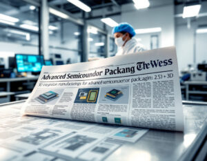
随着晶体管尺寸缩小速度放缓,先进的半导体封装已成为提升系统性能的关键因素。设计人员不再采用大型单芯片,而是将芯片组、存储器堆叠和光子元件组装在硅中介层、有机衬底或玻璃基片上。2.5D 集成将芯片并排放置在共享的中介层上。3D 堆叠则利用硅通孔和混合键合技术,实现小于 10 微米的互连间距。高带宽存储器是目前最显著的商业应用案例。
制造和热限制是主要问题。翘曲、芯片偏移、底部填充物空隙以及热膨胀系数不匹配导致的热机械应力都会降低良率。堆叠逻辑电路的散热以及组装前对已知良品芯片的测试仍然是一个悬而未决的问题。共封装光学器件增加了对准和可靠性方面的问题。以下索引的出版物和专利涉及键合工艺、中介层和基板设计、测试通道、散热解决方案以及芯片间互连标准。
如今,性能提升主要体现在封装方面,因此与客户一起研究封装技术至关重要。基于芯片组的处理器连接到 半导体, FPGA 和 高性能计算需要更好散热路径的功率芯片正在研发中。 宽带隙半导体封装在同一设备上的微型传感器正在涌现。 微机电系统.
这是我们最新精选的全球英文版先进半导体封装出版物和专利,涵盖众多科学在线期刊,并按芯片、2.5D 集成、3D 集成电路、混合键合、硅通孔、硅中介层、扇出型晶圆级封装、重分布层、微凸块、晶圆间键合、芯片间键合、玻璃基板、嵌入式桥接、先进封装、高带宽存储器、共封装光学器件、底部填充、翘曲、导热界面材料和异构集成等领域进行分类和重点介绍。
Probe card device and transition substrate thereof
Patent published on the 2026-11-12 in US under Ref US20260358376 by SILICON FUTURE MANUFACTURING CO LTD [TW] (Sung Wen-tsung [tw], Yu Chia-hsiang [tw], Lin You-chen [tw], Chen Yu-chien [tw], Wu Cheng-chun [tw], Wei Chih-wei [tw])
Abstract: A probe card device comprises: a circuit substrate having a circuit substrate surface; an interposer substrate having a first interposer substrate surface and a second interposer substrate surface opposite to the first interposer substrate surface, the interposer substrate being disposed on the circuit substrate surface and electrically connected to the circuit substrate via a plurality of interposer through-holes; a transition substrate disposed on the second interposer substrate surface and el[...]
Our summary: The probe card device includes a circuit substrate and an interposer substrate with through-holes for electrical connection. A transition substrate is mounted on the interposer substrate, featuring a redistribution layer. The probe head contains a probe substrate with multiple probes connected to the interposer substrate.
probe card, interposer substrate, transition substrate, redistribution layer
Patent
Underfill material, electronic component device, and method for manufacturing electronic component device
Patent published on the 2026-11-12 in WO under Ref WO2026234890 by RESONAC CORP [JP] (Uchiyama Tomomi [jp], Suzuki Takayuki [jp], Yamaura Masashi [jp])
Abstract: An underfill material comprising a radically polymerizable compound and a peroxide having a 10-hour half-life temperature of 90-110° C, the radically polymerizable compound comprising a maleimide compound.[...]
Our summary: This document describes an underfill material for electronic components. The material includes a radically polymerizable compound and a peroxide with a specific half-life temperature. It highlights the use of a maleimide compound in the formulation.
underfill material, electronic component, radically polymerizable compound, manufacturing method
Patent
Display module and display device including same
Patent published on the 2026-11-12 in WO under Ref WO2026235284 by SAMSUNG ELECTRONICS CO LTD [KR] (Oh Jihwan [kr], Kim Sungwook [kr], Hwang Seondeok [kr], Jeong Seungjun [kr], Lee Donghun [kr], Lee Daehee [kr], Park Seeun [kr], Kim Hyungsuk [kr], Kim Jiha [kr])
Abstract: Disclosed herein is a display module. The display module comprises: a glass substrate; a plurality of metal layers disposed on a first surface and a second surface of the glass substrate, respectively; at least one glass through-electrode that electrically connects the plurality of metal layers by passing through the glass substrate; and a plurality of buffer layers respectively disposed between the glass substrate and the plurality of metal layers. The plurality of buffer layers are formed of a[...]
Our summary: The display module includes a glass substrate with metal layers on both surfaces. It features glass through-electrodes connecting the metal layers. Buffer layers with a lower thermal expansion coefficient are placed between the substrate and metal layers.
display module, glass substrate, metal layers, thermal expansion
Patent
Method for manufacturing electronic component device
Patent published on the 2026-11-12 in WO under Ref WO2026234891 by RESONAC CORP [JP] (Uchiyama Tomomi [jp], Suzuki Takayuki [jp], Morimoto Tsuyoshi [jp], Yamaura Masashi [jp])
Abstract: This method for manufacturing an electronic component device includes: filling a gap between an electronic component and a substrate electrically connected to the electronic component via a connection part with an underfill material containing a radical polymerizable compound and a radical polymerization initiator at a temperature lower than a 10-hour half-life temperature of the radical polymerization initiator by 10°C or more; and heating the underfill material to a temperature higher than th[...]
Our summary: This method involves filling a gap between an electronic component and a substrate with an underfill material. The underfill material contains a radical polymerizable compound and initiator, applied at a specific temperature. After filling, the material is heated to cure it effectively.
underfill material, radical polymerization, electronic component, substrate
Patent
Encapsulation structure
Patent published on the 2026-11-12 in US under Ref US20260363130 by AAC MICROTECH CHANGZHOU CO LTD [CN] (Bai Bingyue [cn])
Abstract: [0000] An encapsulation structure, including: a circuit board; a vapor chamber arranged on a first surface of the circuit board, the vapor chamber and the circuit board hermetically defining an accommodating cavity; a chip connected to the circuit board and accommodated in the accommodating cavity, a gap being formed between the chip and the vapor chamber; and a thermal interface material filling in the gap and used for transferring heat generated by the chip to the vapor chamber. A heat conduct[...]
Our summary: An encapsulation structure includes a circuit board and a vapor chamber defining an accommodating cavity. A chip is connected to the circuit board and placed in the cavity, with a gap between the chip and the vapor chamber. Thermal interface material fills the gap, enhancing heat transfer from the chip to the vapor chamber.
encapsulation, circuit board, vapor chamber, thermal interface material
Patent
Wafer-to-wafer bonded computer system with integrated optical circuit switch-enabled redundancy
Patent published on the 2026-11-12 in US under Ref US20260358564 by LIGHTMATTER INC [US] (Kumar Nikhil [us], Srinivasan Srinivasan Ashwyn [ca], Bunandar Darius [us])
Abstract: [0000] Described herein are multi-reticle computer systems based on wafer-to-wafer bonding. A system may include a photonic wafer patterned with a plurality of photonic tiles and a computer wafer patterned with a plurality of computer tiles. The computer wafer may be bonded to the photonic wafer such that each photonic tile is coupled to a corresponding computer tile. Each photonic tile may include a plurality of optical lanes configured to carry optical signals, a plurality of monitoring photod[...]
Our summary: The system integrates photonic and computer wafers through wafer-to-wafer bonding. Each photonic tile monitors optical lanes for defects using photodetectors. In case of a defect, the system redirects light to a backup lane using switches.
wafer-to-wafer bonding, photonic circuits, optical redundancy, computer systems
Patent
Multichromic polymers based on 5-[3,5-di(carbazol-9-yl)phenyl]benzene-1,3-dicarbonitrile and dithiophene derivatives for rapid switching electrochromic devices
Published on 2026-06-23 by Chung-Wen Kuo, Pei-Ying Lee, Pei-Jun Sun, Yuan-Chung Lin, Tzi-Yi Wu @NATURE
Abstract: Polymer Journal, Published online: 23 June 2026; doi:10.1038/s41428-026-01222-0P(dCzCN-co-bTP) copolymers were electrocoated onto ITO-coated glass substrates. A dual-type complementary electrochromic device (ECD) was fabricated using P(dCzCN-co-bTP) as anodically coloring electrochromes and PEDOT as the cathodically coloring electrochrome. The P(dCzCN-co-bTP)/PEDOT ECD revealed a high ΔT (38.0% at 630 nm), a high coloration efficiency (η = 531.4 cm2 C−1 at 630 nm) and a fast swit[...]
Our summary: Multichromic polymers were developed for rapid switching electrochromic devices. The P(dCzCN-co-bTP)/PEDOT device demonstrated a high coloration efficiency and fast switching time. It exhibited distinct color changes from yellow to blue at specified voltages.
multichromic polymers, electrochromic devices, copolymers, coloration efficiency
Publication
photonics to scale AI data centers
Published on 2026-01-30 by Luis Torrijos-Morn, Daniel Prez-Lpez @NATURE npj
Abstract: npj Nanophotonics, Published online: 30 January 2026; doi:10.1038/s44310-025-00105-1The rapid evolution of artificial intelligence (AI) and its high-performance demands on computational systems have significantly impacted modern data center infrastructure. Conventional scaling strategies are approaching physical and economic limits, necessitating innovations in system-level design and networking technologies. Photonics has emerged as a transformative solution, offering unparalleled bandwidth, en[...]
Our summary: Photonics offers a transformative solution for AI data centers by enhancing bandwidth, energy efficiency, and scalability. The paper discusses innovations like co-packaged optics and optical circuit switches to address interconnect challenges. Integration of these technologies can overcome the limitations of traditional electronic systems in modern data center architecture.
photonics, AI, data centers, scalability
Publication