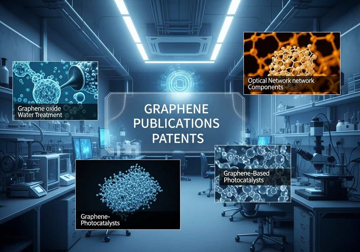
This is our latest selection of worldwide publications and patents in english on Graphene, between many scientific online journals, classified and focused on graphene, wrinklon, straintronic, heterostrain, phonovoltaic, Raman spectroscopy, Klein tunneling, spintronic, chemical vapor deposition, molecular beam epitaxy, Dirac cone and phonon transport.
Publication: pas de nouvelles récentes sur ce sujet particulier. Veuillez essayer la recherche manuelle approfondie dans la base de données des publications dont le lien figure juste au-dessus.
Method for producing graphene
Patent published on the 2025-07-03 in WO under Ref WO2025142960 by AGC INC [JP] (Yoneta Kiyoto [jp], Ono Masashi [jp], Watanabe Hiroshi [jp], Yasui Yoji [jp], Yonemichi Tomohiro [jp])
Abstract: Provided is a method for producing graphene, in which heat bias inside a reaction vessel can be suppressed. Provided is a method for producing graphene using a thermal CVD device, wherein the thermal CVD device has a cylindrical reaction vessel inside of which a base material for graphene production is accommodated, a gas supply unit that is connected to the reaction vessel and supplies a hydrocarbon-containing raw material gas toward the base material, a gas discharge unit that discharges gas[...]
Our summary: Method for producing graphene with suppressed heat bias using a thermal CVD device and a shielding member inside the reaction vessel. Formula provided for optimal raw material gas flow rate based on vessel dimensions.
graphene, method, thermal CVD, reaction vessel
Patent
Thermal cvd apparatus and method for producing graphene
Patent published on the 2025-07-03 in WO under Ref WO2025142961 by AGC INC [JP] (Yoneta Kiyoto [jp], Ono Masashi [jp], Watanabe Hiroshi [jp], Yasui Yoji [jp], Yonemichi Tomohiro [jp])
Abstract: Provided is a thermal CVD apparatus for graphene production capable of suppressing heat unevenness inside a reaction vessel. The thermal CVD device for graphene production comprises: a reaction vessel in which a substrate for graphene production is housed; a gas supply section for supplying a raw material gas containing hydrocarbon; a gas discharge section for discharging gas from the inside of the reaction vessel; a heater for heating the inside of the reaction vessel; and a shielding member [...]
Our summary: Thermal CVD apparatus for producing graphene with heat suppression inside reaction vessel. Includes gas supply section, gas discharge section, heater, and shielding member. Shielding plates with defined aperture ratios for efficient heat transfer control.
thermal CVD, graphene production, apparatus, method
Patent
Thermal cvd device and method for producing graphene
Patent published on the 2025-07-03 in WO under Ref WO2025142959 by AGC INC [JP] (Yoneta Kiyoto [jp], Ono Masashi [jp], Watanabe Hiroshi [jp], Yasui Yoji [jp], Yonemichi Tomohiro [jp])
Abstract: Provided is a thermal CVD device for producing graphene capable of suppressing thermal non-uniformity inside a reaction vessel. The thermal CVD device for producing graphene is provided with: a reaction vessel in which a substrate for producing graphene is accommodated; a gas supply unit that is connected to the reaction vessel and supplies a raw material gas containing a hydrocarbon toward the substrate; a gas discharge unit that is connected on the opposite side to the gas supply unit side a[...]
Our summary: Thermal CVD device for producing graphene with suppressed thermal non-uniformity inside reaction vessel, equipped with gas supply unit, gas discharge unit, heater, and shielding members.
thermal CVD, graphene, device, method
Patent
Carbonaceous material with controlled true density, negative electrode for power storage device, and power storage device
Patent published on the 2025-07-03 in WO under Ref WO2025142598 by KURARAY CO LTD [JP] (Nishimura Naohiro [jp], Hattori Yusaku [jp])
Abstract: The present invention pertains to a carbonaceous material in which: the half-width value of a peak near 1360 cm-1 of a Raman spectrum observed by laser Raman spectroscopy is 200-280 cm-1; the true density obtained by a helium method is 1.30-1.95 g/cc; and the nitrogen element content determined by elemental analysis is 0.5-4.6 mass%.[...]
Our summary: Carbonaceous material with controlled true density, negative electrode for power storage device, and power storage device. The present invention pertains to a carbonaceous material in which: the half-width value of a peak near 1360 cm-1 of a Raman spectrum observed by laser Raman spectroscopy is 200-280 cm-1; the true density obtained by a helium method is 1.30-1.95 g/cc; and the nitrogen element content determined by elemental analysis is 0.5-4.6 mass%.
carbonaceous material, true density, negative electrode, power storage device
Patent
Molybdenum-containing carbonaceous material, negative electrode for power storage device, and power storage device
Patent published on the 2025-07-03 in WO under Ref WO2025142600 by KURARAY CO LTD [JP] (Nishimura Naohiro [jp], Hattori Yusaku [jp])
Abstract: The present invention relates to a carbonaceous material for which the value of the half-value width of the peak in the vicinity of 1360 cm-1 in the Raman spectrum observed by laser Raman spectroscopy is 200-280 cm-1, and for which the molybdenum element content as determined by ICP emission spectroscopy is 0.5-7.5 mass%.[...]
Our summary: Molybdenum-containing carbonaceous material with specific Raman spectrum peak width and molybdenum content for negative electrode in power storage device.
molybdenum, carbonaceous material, negative electrode, power storage device
Patent
Novel compound, precursor composition comprising same, and method for manufacturing thin film using same
Patent published on the 2025-06-26 in WO under Ref WO2025135829 by HANSOL CHEMICAL CO LTD [KR] (Yeom Kyu-hyun [kr], Mun Ki-yeung [kr], Ryu Dae-won [kr], Seok Jang-hyeon [kr])
Abstract: The present invention relates to a precursor composition for vapor deposition capable of depositing a thin film through vapor deposition and, specifically, to: a novel compound that can be applied to atomic layer deposition (ALD) or chemical vapor deposition (CVD) and has excellent reactivity, volatility, and thermal stability; a precursor composition comprising the novel compound; and a method for manufacturing a thin film using the precursor composition.[...]
Our summary: The present invention introduces a novel compound suitable for atomic layer deposition (ALD) or chemical vapor deposition (CVD), along with a precursor composition containing the compound, and a method for manufacturing thin films using this composition.
novel compound, precursor composition, thin film, vapor deposition
Patent