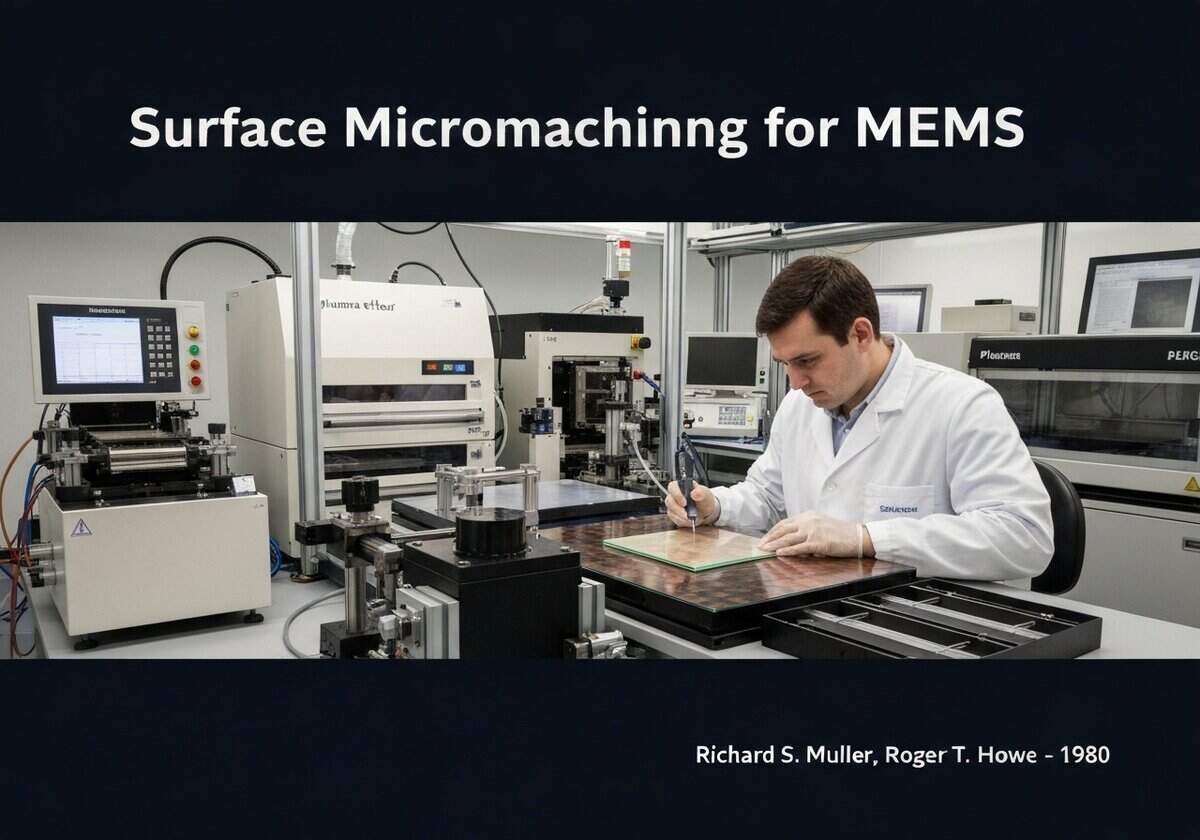
表面マイクロマシニングはMEMS製造の基盤技術であり、基板(通常はシリコンウェハ)上に複雑な機械システムを構築することを可能にする。このプロセスは積層造形であり、構造を層ごとに構築していく。これは、バルクマイクロマシニングの切削加工とは対照的である。典型的なプロセスフローは、窒化ケイ素などの絶縁層を基板上に堆積することから始まる。次に、低圧化学気相成長法(LPCVD)を用いて、リンケイ酸ガラス(PSG)と呼ばれる二酸化ケイ素の一種である犠牲層を堆積する。この層は、フォトリソグラフィとエッチングによってパターン形成され、最終的な構造が基板に固定される領域と、可動部品の下の隙間が定義される。
Next, the structural layer, most commonly polycrystalline silicon (polysilicon), is deposited over the patterned sacrificial layer. This polysilicon layer is then itself patterned to define the geometry of the desired mechanical components, such as beams, gears, or membranes. This sequence of depositing and patterning sacrificial and structural layers can be repeated multiple times to create highly complex, multi-level structures. The final, critical step is the ‘release’ process. The wafer is immersed in a chemical etchant, typically hydrofluoric acid (HF), which selectively removes the sacrificial PSG layers without attacking the polysilicon structural layers or the silicon nitride isolation layer. This leaves the polysilicon structures free to move, suspended above the substrate by their designated anchors.
A major advantage of this technique is its inherent compatibility with standard CMOS integrated circuit manufacturing processes. This allows for the monolithic integration of MEMS devices with their control and signal processing electronics on the same chip, leading to smaller, cheaper, and higher-performance systems. However, surface micromachining is not without its challenges. The primary failure mode during release is ‘stiction,’ where the released structures, once wet, are pulled down to the substrate by capillary forces during drying and become permanently stuck due to intermolecular forces like van der Waals attraction. Various anti-stiction strategies, such as supercritical CO2 drying or special surface coatings, have been developed to mitigate this critical issue.
関連キーワード:表面マイクロマシニング、MEMS、製造、薄膜、ポリシリコン、犠牲層、エッチング、マイクロファブリケーション、リソグラフィー、スティクション。