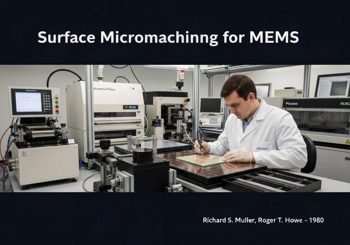
MEMS के लिए सरफेस माइक्रोमशीनिंग
1980
- Richard S. Muller
- Roger T. Howe
सतही माइक्रोमशीनिंग निर्माण MEMS सब्सट्रेट पर पतली फिल्मों को जमा करके और पैटर्न बनाकर उपकरणों का निर्माण किया जाता है। इसमें एक बलिदानी परत (जैसे सिलिकॉन डाइऑक्साइड) जमा करना, उस पर पैटर्न बनाना, एक संरचनात्मक परत (जैसे पॉलीसिलिकॉन) जमा करना और अंत में यांत्रिक संरचना को मुक्त करने के लिए बलिदानी परत को हटाना शामिल है। यह प्रक्रिया वेफर की सतह पर सीधे जटिल, स्वतंत्र सूक्ष्म संरचनाओं के निर्माण की अनुमति देती है।
सतही माइक्रोमशीनिंग, एमईएमएस निर्माण का एक महत्वपूर्ण हिस्सा है, जो सिलिकॉन वेफर जैसे सब्सट्रेट पर जटिल यांत्रिक प्रणालियों के निर्माण को संभव बनाता है। यह प्रक्रिया योगात्मक है, जिसमें संरचनाओं का निर्माण परत दर परत किया जाता है, जो बल्क माइक्रोमशीनिंग की घटावात्मक प्रकृति से भिन्न है। एक सामान्य प्रक्रिया प्रवाह सब्सट्रेट पर सिलिकॉन नाइट्राइड जैसी एक पृथक्करण परत के जमाव से शुरू होता है। इसके बाद, कम दबाव रासायनिक वाष्प जमाव (एलपीसीवीडी) का उपयोग करके एक बलिदानी परत, जो अक्सर फॉस्फोसिलिकेट ग्लास (पीएसजी) नामक सिलिकॉन डाइऑक्साइड का एक प्रकार होती है, जमा की जाती है। फिर इस परत को फोटोलिथोग्राफी और नक़्क़ाशी का उपयोग करके पैटर्न किया जाता है, जिससे उन क्षेत्रों को परिभाषित किया जाता है जहां अंतिम संरचना सब्सट्रेट से जुड़ी होगी और गतिशील भागों के नीचे के अंतराल को भी परिभाषित किया जाता है।
Next, the structural layer, most commonly polycrystalline silicon (polysilicon), is deposited over the patterned sacrificial layer. This polysilicon layer is then itself patterned to define the geometry of the desired mechanical components, such as beams, gears, or membranes. This sequence of depositing and patterning sacrificial and structural layers can be repeated multiple times to create highly complex, multi-level structures. The final, critical step is the ‘release’ process. The wafer is immersed in a chemical etchant, typically hydrofluoric acid (HF), which selectively removes the sacrificial PSG layers without attacking the polysilicon structural layers or the silicon nitride isolation layer. This leaves the polysilicon structures free to move, suspended above the substrate by their designated anchors.
A major advantage of this technique is its inherent compatibility with standard CMOS integrated circuit manufacturing processes. This allows for the monolithic integration of MEMS devices with their control and signal processing electronics on the same chip, leading to smaller, cheaper, and higher-performance systems. However, surface micromachining is not without its challenges. The primary failure mode during release is ‘stiction,’ where the released structures, once wet, are pulled down to the substrate by capillary forces during drying and become permanently stuck due to intermolecular forces like van der Waals attraction. Various anti-stiction strategies, such as supercritical CO2 drying or special surface coatings, have been developed to mitigate this critical issue.
UNESCO Nomenclature: 3313
औद्योगिक इंजीनियरिंग
शगुन
- सेमीकंडक्टर उद्योग से फोटोलिथोग्राफी तकनीकें
- पतली फिल्म के विकास के लिए रासायनिक वाष्प निक्षेपण (सीवीडी)
- गीली और सूखी नक़्क़ाशी प्रक्रियाएँ
- एकीकृत परिपथ (आईसी) निर्माण प्रौद्योगिकी
आवेदन
- प्रोजेक्टरों में डिजिटल माइक्रोमिरर डिवाइस (डीएमडी)
- स्मार्टफ़ोन में जड़त्वीय सेंसर (एक्सेलरोमीटर और जाइरोस्कोप)
- दबाव सेंसर
- इंकजेट प्रिंटर हेड
- आरएफ एमईएमएस स्विच
संभावित नवाचार विचार
बॉट ट्रैफिक को कम करने के कारण, जो वर्तमान में प्रति दिन 40,000 से अधिक है, यह सामग्री केवल समुदाय के सदस्यों के लिए आरक्षित है।
> लॉगिन < या > रजिस्टर < इस सामग्री और अन्य सभी प्रतिबंधित सामग्रियों और उपकरणों तक पहुंच (100% निःशुल्क) है।
Related to: surface micromachining, MEMS, fabrication, thin film, polysilicon, sacrificial layer, etching, microfabrication, lithography, stiction.