Microlavorazione superficiale per MEMS
1980
- Richard S. Muller
- Roger T. Howe
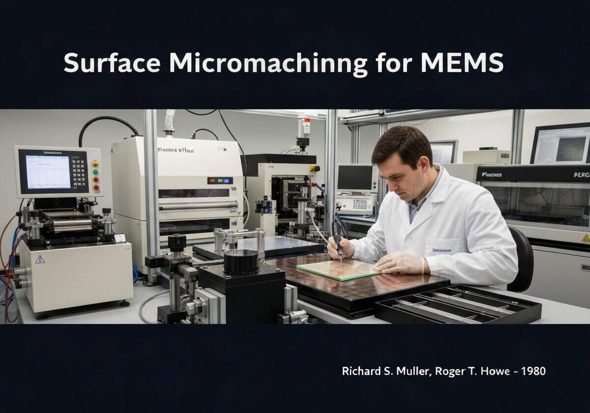
La microlavorazione superficiale costruisce MEMS dispositivi mediante la deposizione e la modellazione di film sottili su un substrato. Il processo prevede una sequenza di fasi: deposizione di uno strato sacrificale (come il biossido di silicio), modellazione dello stesso, deposizione di uno strato strutturale (come il polisilicio) e, infine, rimozione dello strato sacrificale per liberare la struttura meccanica. Questo processo consente la creazione di microstrutture complesse e autoportanti direttamente sulla superficie del wafer.
Surface micromachining is a cornerstone of MEMS fabrication, enabling the creation of intricate mechanical systems on top of a substrate, typically a silicon wafer. The process is additive, building structures layer by layer, which contrasts with the subtractive nature of bulk micromachining. A typical process flow begins with the deposition of an isolation layer, like silicon nitride, on the substrate. Following this, a sacrificial layer, often a type of silicon dioxide called phosphosilicate glass (PSG), is deposited using Low-Pressure Chemical Vapor Deposition (LPCVD). This layer is then patterned using photolithography and etching, defining the areas where the final structure will be anchored to the substrate and the gaps beneath moving parts.
Next, the structural layer, most commonly polycrystalline silicon (polysilicon), is deposited over the patterned sacrificial layer. This polysilicon layer is then itself patterned to define the geometry of the desired mechanical components, such as beams, gears, or membranes. This sequence of depositing and patterning sacrificial and structural layers can be repeated multiple times to create highly complex, multi-level structures. The final, critical step is the ‘release’ process. The wafer is immersed in a chemical etchant, typically hydrofluoric acid (HF), which selectively removes the sacrificial PSG layers without attacking the polysilicon structural layers or the silicon nitride isolation layer. This leaves the polysilicon structures free to move, suspended above the substrate by their designated anchors.
A major advantage of this technique is its inherent compatibility with standard CMOS integrated circuit manufacturing processes. This allows for the monolithic integration of MEMS devices with their control and signal processing electronics on the same chip, leading to smaller, cheaper, and higher-performance systems. However, surface micromachining is not without its challenges. The primary failure mode during release is ‘stiction,’ where the released structures, once wet, are pulled down to the substrate by capillary forces during drying and become permanently stuck due to intermolecular forces like van der Waals attraction. Various anti-stiction strategies, such as supercritical CO2 drying or special surface coatings, have been developed to mitigate this critical issue.
UNESCO Nomenclature: 3313
- Ingegneria industriale
Precursori
- photolithography techniques from the semiconductor industry
- deposizione chimica da vapore (CVD) per la crescita di film sottili
- wet and dry etching processes
- integrated circuit (IC) fabrication technology
Applicazioni
- digital micromirror devices (DMDs) in projectors
- inertial sensors (accelerometers and gyroscopes) in smartphones
- sensori di pressione
- inkjet printer heads
- RF MEMS switches
Idee e potenziali innovazioni
A causa dell'eliminazione del traffico generato dai bot, che attualmente supera i 40.000 al giorno, questo contenuto è riservato ai membri della community.
> Accedi O > Registrati L'accesso a questo contenuto, così come a tutti gli altri contenuti e strumenti riservati, è (100% gratuito).
Related to: surface micromachining, MEMS, fabrication, thin film, polysilicon, sacrificial layer, etching, microfabrication, lithography, stiction.