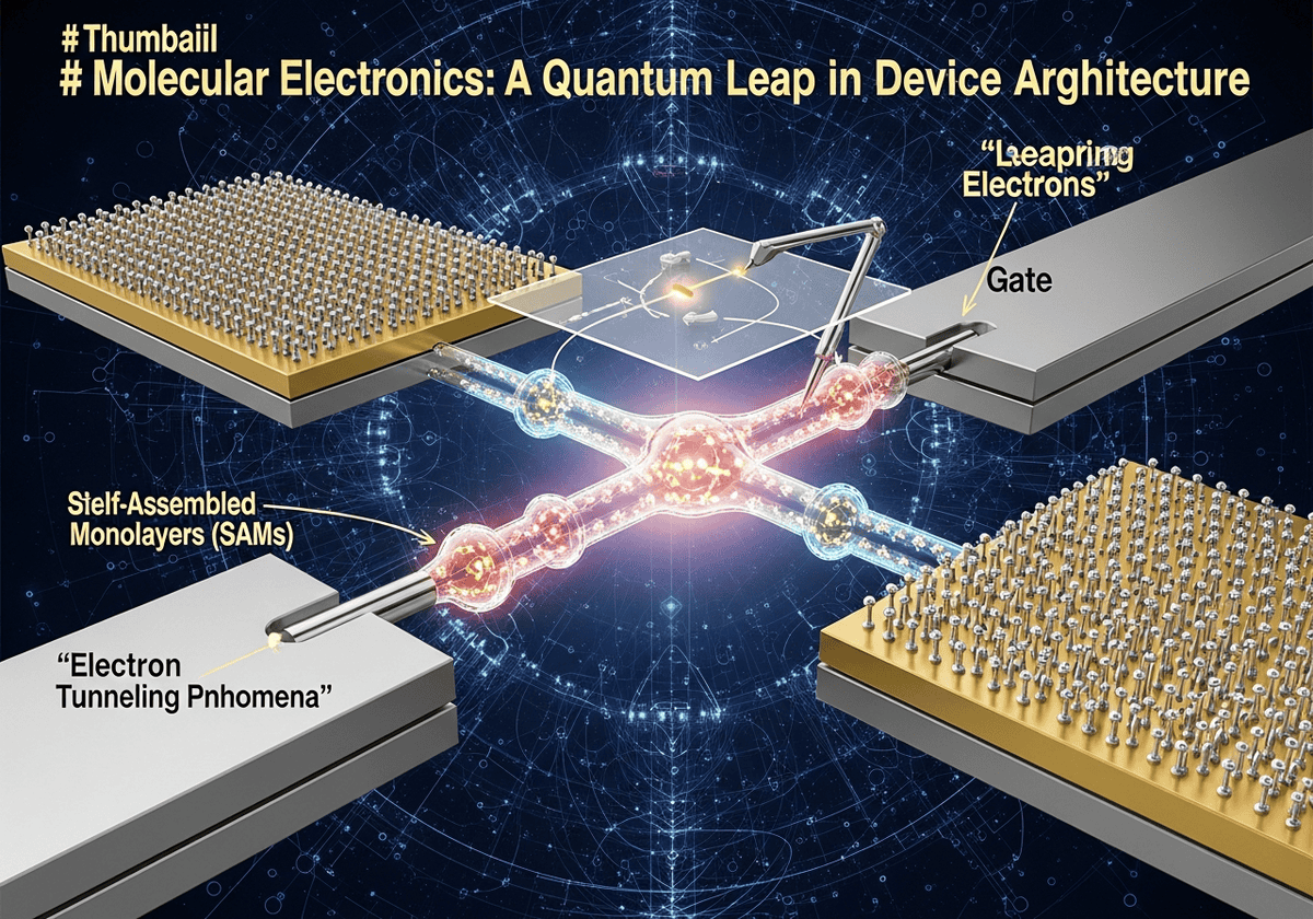

Molecular Electronics explores charge transport and electronic functionality at the scale of individual molecules and molecular assemblies, integrating principles of quantum mécanique, organic chemistry, and nanofabrication. Central topics include molecular junctions, self-assembled monolayers, single-molecule transistors, and electron tunneling phenomena, with emphasis on controlling conductance, switching behavior, and spin-dependent effects. Research advances focus on molecular wires, rectifiers, switches, and memory elements, employing techniques such as scanning tunneling microscopy and break junctions to characterize electronic properties. Our following collection compiles the most recent peer-reviewed articles and patents, highlighting innovations in device architectures, molecular synthesis, and measurement methodologies driving the miniaturization of electronic components beyond conventional semiconductor technology.
Voici notre dernière sélection de publications et brevets mondiaux en anglais sur l'électronique moléculaire, parmi de nombreuses revues scientifiques en ligne, classés et axés sur la jonction moléculaire, la monocouche auto-assemblée, le transistor à molécule unique, la mesure de conductance, le transport d'électrons, le fil moléculaire, l'effet tunnel quantique, la molécule redox, la microscopie à effet tunnel, la technique de rupture de jonction, le porteur de charge, le commutateur moléculaire, l'électrode à nanogap, la spintronique, le redresseur moléculaire, le semi-conducteur organique, l'orbitale moléculaire, le couplage électron-phonon, la spintronique moléculaire, l'interférence quantique, la diode moléculaire, l'électromigration, le nanopore, l'assemblage moléculaire, la résonance plasmon de surface, le transfert d'électrons, la conductance moléculaire, le nanocircuit moléculaire, la mémoire moléculaire et l'optoélectronique moléculaire.
Perovskite solar cell and tandem solar cell comprising same
Patent published on the 2026-07-02 in WO under Ref WO2026142030 by HANWHA SOLUTIONS CORP [KR] (Jung Dong Ki [kr], Jang Eun Soo [kr], Moon Chan Su [kr], Choi In Take [kr])
Abstract: An embodiment of the present invention relates to a perovskite solar cell and a tandem solar cell comprising same, the perovskite solar cell comprising: a substrate; a first electrode disposed on the substrate; a second electrode disposed to face the first electrode; a light-absorbing layer disposed between the first electrode and the second electrode; and a hole transport layer between the second electrode and the light-absorbing layer, wherein the hole transport layer comprises a self-assemble[...]
Our summary: The invention describes a perovskite solar cell featuring a substrate, electrodes, and a light-absorbing layer. It includes a hole transport layer made of self-assembled organic material. This design enhances the performance of the solar cell device.
Perovskite, tandem solar cell, self-assembled monolayer, hole transport layer
Patent
Semiconductor device and method of manufacturing the same
Patent published on the 2026-07-02 in US under Ref US20260190520 by TAIWAN SEMICONDUCTOR MANUFACTURING CO LTD [TW] (Jiang Sin-yi [tw], Chen Sung-wen Huang [tw], Chu Yi-shin [tw], Chen Hsiang-lin [tw], Lin Jung-i [tw], Liu Jen-cheng [tw], Lin Hsing-chih [tw], Liao Yin-kai [tw])
Abstract: Some embodiments relate to an image-sensor integrated circuit (IC) that includes an array of avalanche photodiode (APD) elements. A first APD element of the array of APD elements includes an absorption region having a germanium semiconductor and a multiplication region including a diode of a silicon semiconductor. The absorption region is configured to generate a charge carrier in response to an incident photon. The multiplication region is configured to generate an avalanche current of charge c[...]
Our summary: The content discusses a semiconductor device that features an array of avalanche photodiodes (APDs). It describes the structure of the first APD element, including its absorption and multiplication regions made of germanium and silicon, respectively. The device is designed to generate charge carriers in response to incident photons and produce an avalanche current.
Avalanche photodiode, Image sensor, Semiconductor manufacturing, Charge carrier generation
Patent
Imaging element and imaging device
Patent published on the 2026-07-02 in WO under Ref WO2026141651 by NIKON CORP [JP] (Takagi Toru [jp])
Abstract: This imaging element comprises: a first substrate that has a first photoelectric conversion unit which converts light into electric charge and which is formed of a first inorganic semiconductor material; and a second substrate that is laminated together with the first substrate and has a second photoelectric conversion unit which is formed of a second inorganic semiconductor material different from the first inorganic semiconductor material and which converts, into electric charge, light that ha[...]
Our summary: The imaging element includes a first substrate with a photoelectric conversion unit made of a first inorganic semiconductor. A second substrate is laminated with the first and contains a second photoelectric conversion unit from a different inorganic semiconductor. This unit converts light that has passed through the first unit into electric charge.
photoelectric conversion, inorganic semiconductor, imaging element, imaging device
Patent
Organic electroluminescent material and device
Patent published on the 2026-07-02 in US under Ref US20260190602 by BEIJING SUMMER SPROUT TECH CO LTD [CN] (Zhang Xuan [cn], Kwong Chi Yuen Raymond [cn], Li Feng [cn], Xia Chuanjun [cn], Wang Yang [cn])
Abstract: [0000] Provided are an organic electroluminescent material and device. The organic electroluminescent material is a compound having a structure of Formula 1. The compound may be used as a host material, an electron transporting material, or a hole blocking material in an organic electroluminescent device and can greatly improve device performance, for example, improve device efficiency and achieve an unexpectedly significant improvement in device lifetime. Further provided are an organic electro[...]
Our summary: The document discusses an organic electroluminescent material and device. The material can function as a host, electron transport, or hole-blocking component. It significantly enhances device efficiency and lifetime.
Organic electroluminescence, device performance, host material, compound composition
Patent
Confinement-controlled redox behavior in viologen-functionalized polymer brushes
Published on 2026-06-18 by Hongyao Zhou, Hiromu Moku, Koshiro Tamashima, Mizuha Ujita, Masayuki Morimoto, Hitoshi Asakawa, Teppei Yamada @NATURE
Abstract: Polymer Journal, Published online: 18 June 2026; doi:10.1038/s41428-026-01221-1Viologen-functionalized polymer brushes exhibit fundamentally different electrochemical behaviors than their solution-phase counterparts. In solution, poly(4-vinylpyridine-N-diethylviologen) (P4VP-V) undergoes reversible coil–globule transitions upon reduction, with cyclic voltammetry revealing cooperative multielectron transfer driven by radical dimerization. When confined as a surface-grafted brush on ITO, chain c[...]
Our summary: Viologen-functionalized polymer brushes show distinct electrochemical behaviors compared to their solution-phase forms. In a confined environment, chain crowding limits radical dimerization, leading to single-electron redox processes. This study highlights the impact of nanoscale confinement on electron-transfer behavior in redox-active polymers.
Viologen, Polymer brushes, Redox behavior, Electrochemistry
Publication
Efficient and stable cis-isomerization method for lycopene
Patent published on the 2026-06-18 in WO under Ref WO2026124395 by CHINA PHARMACEUTICAL UNIV [CN] (Nian Linyu [cn], Cao Chongjiang [cn])
Abstract: Disclosed in the present invention is an efficient and stable cis-isomerization method for lycopene. The method comprises using a bimetallic metal-organic framework material as a catalyst to catalyze the cis-isomerization of lycopene. In the method, confined water molecules can also be added to a reaction system as a catalytic medium to efficiently catalyze the isomerization of lycopene. The catalyst attacks and activates a conjugated double bond of all-trans-lycopene in an electron-rich environ[...]
Our summary: The invention presents a method for the efficient cis-isomerization of lycopene using a bimetallic metal-organic framework catalyst. Confined water molecules enhance the reaction by acting as an electron transfer medium. The process achieves an isomerization efficiency of 82.2% and a retention rate of 90.3% for lycopene.
cis-isomerization, lycopene, bimetallic catalyst, green chemistry
Patent
Water electrolyzer with cation exchange membrane
Patent published on the 2026-06-18 in US under Ref US20260168115 by VOLTA ENERGY INC [US] (Emerick Patrick [us], Puranam Srivatsava V [ca], Iyer Raghavendra [us], Datta Ravindra [us])
Abstract: [0000] An alkaline water electrolyzer (AWE) incorporates a cation-exchange membrane (CEM) instead of a conventional porous diaphragm or an anion-exchange membrane used in the conventional AWE. The corresponding change in the nature of the charge carrier from the hydroxyl anion (OH) in the conventional AWE to an alkali cation (A) has a substantial effect on the electrochemistry and performance of the resulting CEM-alkaline water electrolyzer (CEM-AWE). The water electrolysis device combines advan[...]
Our summary: The CEM-AWE utilizes a cation-exchange membrane, enhancing electrochemical performance. It merges benefits from liquid alkaline and proton-exchange membrane technologies. This novel design employs non-PGM catalysts, improving efficiency and longevity.
Cation exchange membrane, alkaline water electrolyzer, electrochemistry, non-PGM catalysts
Patent
assessing the robustness of topological insulating states against realistic structural defects
Published on 2026-04-24 by Shuoke Xu, Wenjin Gao, Pengfei Yu, Guo-Xiang Zhi, Ke Xu, Yujing Zhang and Miao Zhou @IOP SCIENCE
Abstract: Two-dimensional topological insulator, or quantum spin Hall (QSH) insulator, holds topologically protected edge states with significant implications for diverse fields, yet the robustness against realistic structural defects remains elusive. Here, by combining first-principles calculations, ab initio molecular dynamics (AIMD) and Monte Carlo simulations, we consider Bi(111) bilayer–a large-gap QSH insulator–under ion irradiation, and explore the topological robustness with the generated defe[...]
Our summary: This study investigates the robustness of two-dimensional topological insulators against structural defects. Using first-principles calculations and simulations, it identifies dominant defects and their impact on topological edge states. The findings highlight the limitations of QSH insulators in practical applications under defect conditions.
topological insulators, quantum spin Hall, structural defects, first-principles calculations
Publication