Heim » Top-Down Nanomaterial Synthesis

Top-Down Nanomaterial Synthesis

1970
Researcher operating ball mill for top-down nanomaterial synthesis in a cleanroom.

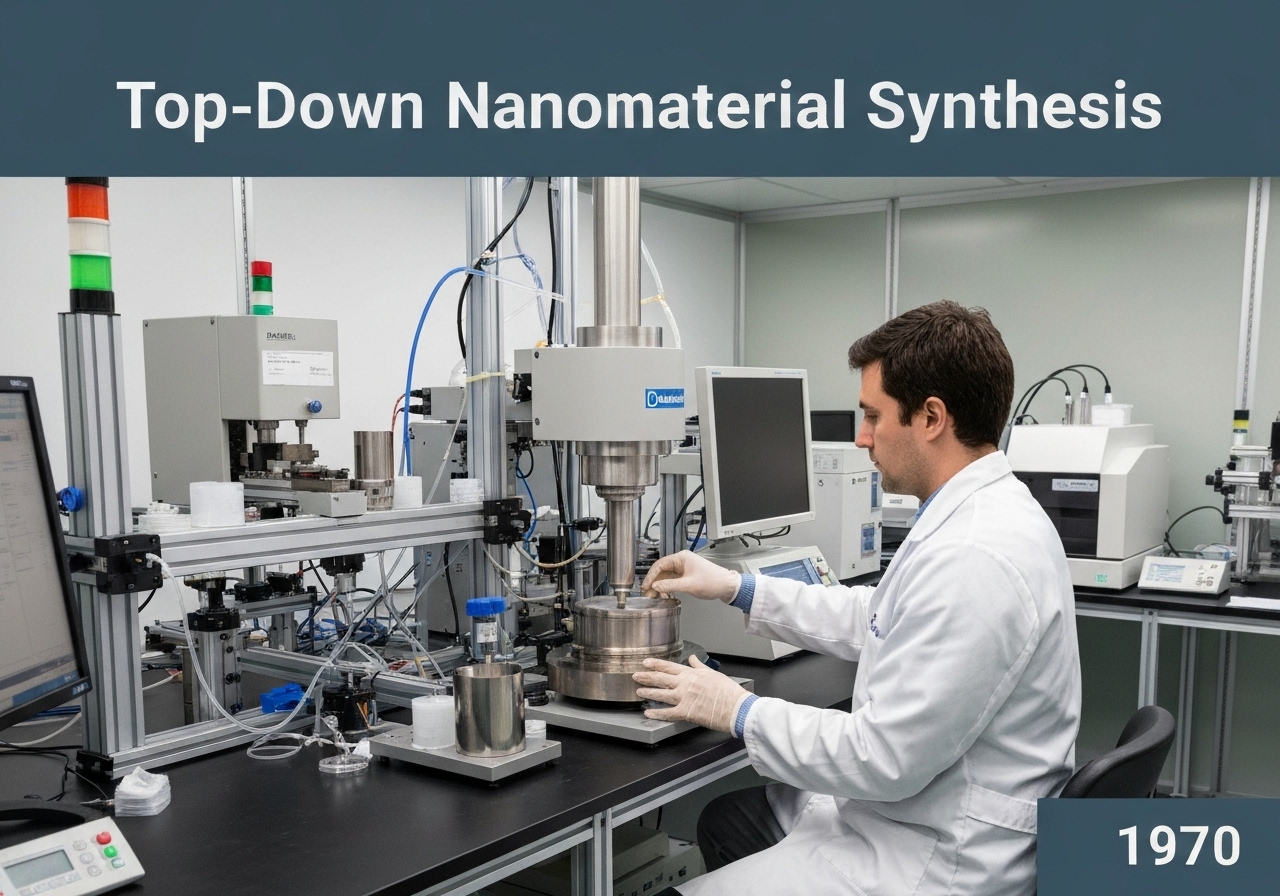
Top-down synthesis involves creating nanomaterials by starting with a larger, bulk material and breaking it down or patterning it to the nanoscale. Key techniques include mechanical methods like ball milling and lithographic methods like photolithography, electron-beam lithography, and nanoimprint lithography. These methods are often used for creating structured surfaces and integrated circuits, but can suffer from surface imperfections.

Top-down approaches are conceptually straightforward: they are an extension of traditional microfabrication techniques to smaller dimensions. The most prominent example is lithography, the cornerstone of the semiconductor industry. In photolithography, a light-sensitive polymer (photoresist) is coated onto a substrate. A mask is used to selectively expose the resist to UV light, causing a chemical change that allows for the selective removal of either the exposed or unexposed regions. The underlying material can then be etched or deposited upon, transferring the pattern from the mask to the substrate. To achieve nanoscale features, shorter wavelength light sources (e.g., extreme ultraviolet, EUV) or alternative patterning sources like electron beams (e-beam lithography) are used. E-beam lithography offers very high resolution but is a slow, serial process, making it unsuitable for mass production but excellent for prototyping and mask making.

Another major class of top-down methods is mechanical attrition. High-energy ball milling, for instance, places a bulk material in a container with hard grinding media (balls). The container is rotated at high speed, causing the balls to collide with and fracture the material, progressively reducing its particle size down to the nanometer scale. This Verfahren is simple and scalable for producing large quantities of nanopowders but offers poor control over particle shape and size distribution, and can introduce impurities from the milling media.

The primary advantage of top-down methods, particularly lithography, is the ability to create precisely ordered and complex structures over large areas, which is essential for integrated circuits. However, a significant drawback is the introduction of crystallographic damage and surface defects during the etching or milling process, which can negatively impact the material’s properties.

UNESCO Nomenclature: 2211
– Solid state physics

Typ

Chemical Process

Disruption

Incremental

Verwendung

Widespread Use

Precursors

  • invention of the printing press and early lithographic printing
  • development of photography and photosensitive chemicals
  • the invention of the transistor and the subsequent drive for miniaturization in electronics
  • advances in vacuum technology and plasma physics for etching processes

Anwendungen

  • manufacturing of computer microprocessors and memory chips
  • fabrication of microelectromechanical systems (mems)
  • creation of patterned surfaces for biomedical applications
  • production of nanopowders for ceramics and composites
  • fabrication of molds for nanoimprint lithography

Patente:

DAS

Potential Innovations Ideas

!Professionals (100% free) Mitgliedschaft erforderlich

Sie müssen ein Professionals (100% free) Mitglied sein, um auf diesen Inhalt zugreifen zu können.

Jetzt teilnehmen

Sie sind bereits Mitglied? Hier einloggen
Related to: top-down synthesis, lithography, photolithography, e-beam lithography, ball milling, microfabrication, semiconductor, etching, nanopatterning, mems.

Schreibe einen Kommentar

Deine E-Mail-Adresse wird nicht veröffentlicht. Erforderliche Felder sind mit * markiert

VERFÜGBAR FÜR NEUE HERAUSFORDERUNGEN
Mechanical Engineer, Project, Process Engineering or R&D Manager
Effektive Produktentwicklung

Kurzfristig für eine neue Herausforderung verfügbar.
Kontaktieren Sie mich auf LinkedIn
Plastic metal electronics integration, Design-to-cost, GMP, Ergonomics, Medium to high-volume devices & consumables, Lean Manufacturing, Regulated industries, CE & FDA, CAD, Solidworks, Lean Sigma Black Belt, medical ISO 13485

Wir suchen einen neuen Sponsor


Ihr Unternehmen oder Ihre Institution beschäftigt sich mit Technik, Wissenschaft oder Forschung?
> Senden Sie uns eine Nachricht <

Erhalten Sie alle neuen Artikel
Kostenlos, kein Spam, E-Mail wird nicht verteilt oder weiterverkauft

oder Sie können eine kostenlose Vollmitgliedschaft erwerben, um auf alle eingeschränkten Inhalte zuzugreifen >Hier<

Historical Context

(if date is unknown or not relevant, e.g. "fluid mechanics", a rounded estimation of its notable emergence is provided)

Related Invention, Innovation & Technical Principles

Nach oben scrollen

Das gefällt dir vielleicht auch