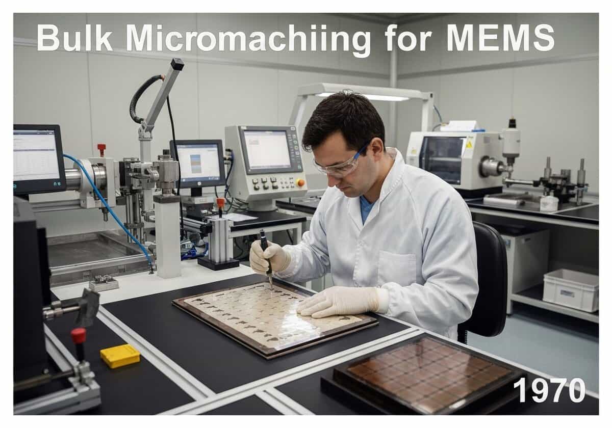
Mikrobearbeitung in großen Mengen für MEMS
Die Mikrobearbeitung in großen Mengen ist ein subtraktives Fertigungsverfahren, das erzeugt MEMS Strukturen werden durch selektives Ätzen eines Substrats, typischerweise eines Siliziumwafers, erzeugt. Dabei kommen Nass- oder Trockenätzverfahren zum Einsatz, um das Material zu formen. Anisotrope Ätzmittel wie Kaliumhydroxid (KOH) sind weit verbreitet, da sie verschiedene Kristallflächen des Siliziums unterschiedlich schnell ätzen und so die Herstellung präziser V-förmiger Nuten und Vertiefungen ermöglichen.
Die Mikrobearbeitung von Bauelementen ist eine der ältesten und etabliertesten Methoden zur Herstellung von MEMS. Als subtraktives Verfahren werden die Strukturen des Bauelements direkt aus dem Substrat, üblicherweise einem einkristallinen Siliziumwafer, herausgearbeitet. Die Technik basiert maßgeblich auf dem Ätzen, das sich grob in nasschemisches (chemisches) und trockenes (plasmabasiertes) Ätzen unterteilen lässt.
Wet etching is the more traditional approach. It can be isotropic, etching at the same rate in all directions, which results in rounded, undercut features. More commonly for MEMS, anisotropic wet etching is used. This method exploits the fact that the etch rate in single-crystal silicon depends on the crystallographic orientation. Etchants like potassium hydroxide (KOH), tetramethylammonium hydroxide (TMAH), and ethylenediamine pyrocatechol (EDP) etch the (100) and (110) crystal planes much faster than the (111) planes. By aligning the mask pattern with the crystal axes on a (100)-oriented wafer, this property can be used to create precisely defined structures with angled sidewalls, such as V-grooves for fiber optics or pyramidal pits. The (111) planes act as natural etch-stops, allowing for excellent control over the final geometry. Diaphragms for pressure sensors are a classic application, formed by etching from the backside of a wafer until an etch-stop layer (like a heavily doped boron layer or an electrochemical stop at a p-n junction) is reached.
Dry etching, particularly Deep Reactive-Ion Etching (DRIE), has become a dominant bulk micromachining technique. DRIE allows for the creation of very deep, high-aspect-ratio structures with nearly vertical sidewalls, something not possible with wet etching. The most common method is the ‘Bosch process,’ which alternates between an etching step (using a plasma like SF6) and a passivation step (using a polymerizing gas like C4F8). The passivation layer protects the sidewalls from being etched, forcing the etch to proceed primarily in the vertical direction. This cycle is repeated hundreds or thousands of times to achieve depths of hundreds of microns. DRIE is essential for manufacturing modern high-performance inertial sensors, microfluidic devices, and through-silicon vias (TSVs) for 3D chip stacking.
UNESCO Nomenclature: 3313
- Wirtschaftsingenieurwesen
Verwendung
Weitverbreitete Verwendung
Vorläufer
- crystal orientation knowledge in silicon wafers
- development of chemical etchants for silicon
- photolithography for pattern definition
- masking materials resistant to etchants (e.g., silicon nitride)
Anwendungen
- pressure sensor diaphragms
- inkjet printer nozzles
- microfluidic channels
- atomic force microscope (AFM) cantilevers
- v-grooves for optical fiber alignment
Potenzielle Innovationsideen
Aufgrund des hohen Datenverkehrs durch Web-Scraping-Bots, der derzeit mehr als 40.000 Anfragen pro Tag umfasst, ist dieser Inhalt ausschließlich Community-Mitgliedern vorbehalten.
> Anmelden < oder > Registrieren < (100% kostenlos) Zugriff darauf sowie auf alle anderen eingeschränkten Inhalte und Tools.
Verwandte Themen: Volumenmikrobearbeitung, MEMS, Ätzen, Silizium, anisotropes Ätzen, KOH, DRIE, Tiefenreaktives Ionenätzen, subtraktives Verfahren, Mikrofertigung.