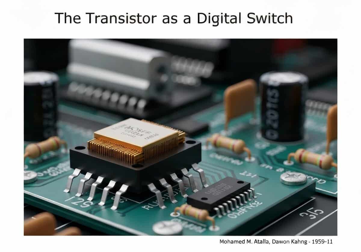
In digital applications, a MOSFET is operated in its cutoff (off) and triode/saturation (on) regions. When the gate voltage is below a certain threshold, the channel is non-conductive, the switch is ‘off’, and it represents a logic ‘0’. When the gate voltage is above the threshold, the channel becomes conductive, the switch is ‘on’, and it represents a logic ‘1’. By combining MOSFETs, typically in a complementary pair of P-type and N-type (forming CMOS logic), all basic logic gates can be constructed. The ability to miniaturize MOSFETs, as described by Moore’s Law, has driven the exponential growth in computing power for over half a century.