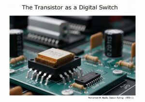
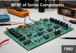
PCB의 단락, 개방 회로, 저항, 용량 및 기타 기본 물리량을 검사하는 자동화 테스트입니다. 부품이 기판에 납땜된 후 수행되며 제조 결함을 식별하는 데 사용됩니다.
장점
PCB를 빠르고 효율적으로 테스트할 수 있으며, 다양한 제조 결함을 감지할 수 있습니다.
단점
설치 및 유지 관리 비용이 많이 들 수 있으며, 보드의 모든 구성 요소를 테스트할 수 없을 수도 있습니다.
카테고리:
조작, 품질
다음과 같은 경우에 가장 적합합니다:
대량 생산 환경에서 인쇄 회로 기판의 품질을 테스트합니다.
In-Circuit Testing (ICT) can be particularly advantageous in industries such as consumer electronics, automotive, and medical devices, where high reliability and performance of printed circuit boards are paramount. The methodology is typically integrated during the production processes of PCB manufacturing, specifically in the later phases where components have been soldered but prior to final assembly. This context allows for the rapid identification and rectification of issues such as solder bridging, incorrect component placements, or open circuits, which could otherwise lead to product failures. Key participants in this testing process include test engineers who design the test fixtures and programs, as well as manufacturing technicians responsible for operating the ICT equipment. The integration of ICT into a production line not only promotes quality assurance but also enhances manufacturing yields, as defects can be tackled before the product undergoes further assembly or incurs additional costs in later stages. Moreover, with automated testing protocols, ICT can provide consistent results that support high-volume production environments, making it suitable for any production scale, from prototyping phases to mass production. As industries increasingly push for edge cases like miniaturization and complex circuitry, ICT can adapt by incorporating advanced functionalities such as boundary-scan testing for digital design verification, further enhancing its utility in robust testing scenarios.
이 방법론의 주요 단계
ICT 테스트 픽스처를 PCB에 연결하십시오.
ICT 소프트웨어를 초기화하고 특정 PCB 설계에 대한 테스트 매개변수를 구성합니다.
연결부 사이의 단락 및 개방 회로를 확인하기 위해 연속성 테스트를 수행하십시오.
저항을 측정하고 지정된 범위 내에 있는지 확인하십시오.
정전 용량 값을 사전 정의된 기준과 비교하여 확인하십시오.
구성 요소의 작동 및 응답을 확인하기 위해 기능 테스트를 수행합니다.
테스트 결과를 기록하고 실패 사례는 추가 분석을 위해 표시합니다.
테스트 프로그램의 효율성과 설계 범위 준수 여부를 검토하십시오.
프로 팁
정확한 연결과 신뢰할 수 있는 테스트 결과를 보장하려면 고품질의 정밀 프로브에 투자하십시오.
테스트 픽스처 설계를 최적화하여 오탐을 최소화하고 다양한 PCB 레이아웃에 맞게 쉽게 재구성할 수 있도록 합니다.
시험 결과에 대한 데이터 분석을 구현하여 반복적으로 발생하는 결함을 파악하고 제조 공정을 지속적으로 개선합니다.