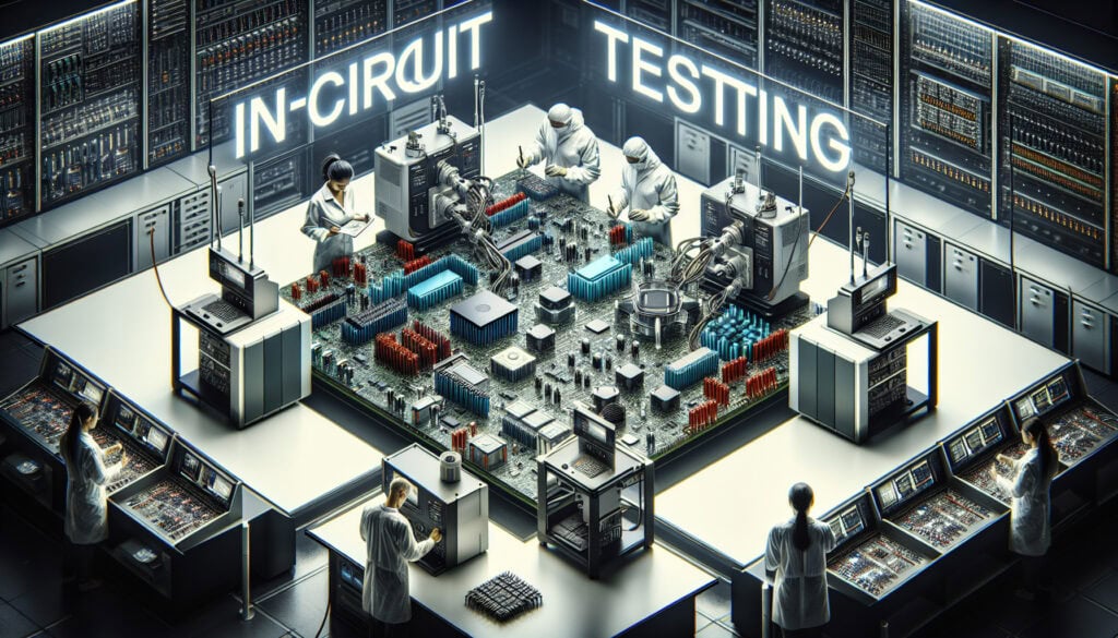
In-Circuit Testing (ICT) can be particularly advantageous in industries such as consumer electronics, automotive, and medical devices, where high reliability and performance of printed circuit boards are paramount. The methodology is typically integrated during the production processes of PCB manufacturing, specifically in the later phases where components have been soldered but prior to final assembly. This context allows for the rapid identification and rectification of issues such as solder bridging, incorrect component placements, or open circuits, which could otherwise lead to product failures. Key participants in this testing process include test engineers who design the test fixtures and programs, as well as manufacturing technicians responsible for operating the ICT equipment. The integration of ICT into a production line not only promotes quality assurance but also enhances manufacturing yields, as defects can be tackled before the product undergoes further assembly or incurs additional costs in later stages. Moreover, with automated testing protocols, ICT can provide consistent results that support high-volume production environments, making it suitable for any production scale, from prototyping phases to mass production. As industries increasingly push for edge cases like miniaturization and complex circuitry, ICT can adapt by incorporating advanced functionalities such as boundary-scan testing for digital design verification, further enhancing its utility in robust testing scenarios.