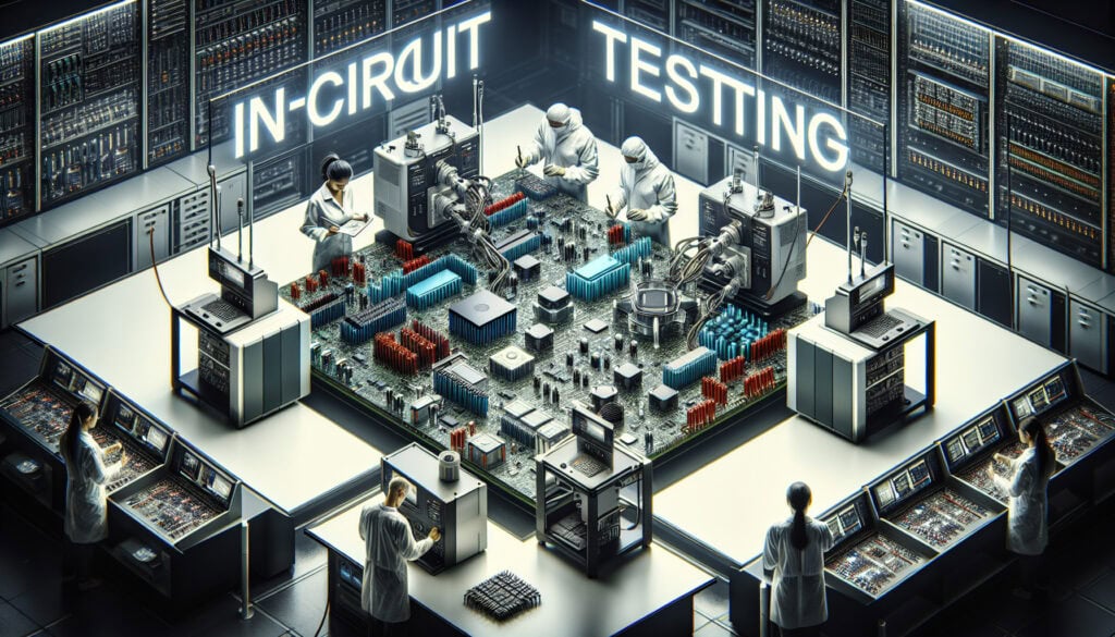
To test the integrity of electronic components on a printed circuito impreso (PCB).
- Metodologías: Economía, Lean Sigma, Fabricación, Resolución de problemas, Calidad
Pruebas en circuito (ICT)
Pruebas en circuito (ICT)
- Ingeniería eléctrica, Resistencia eléctrica, Ingeniería Electrónica, Electrónica, Placa de circuito impreso (PCB), Seguro de calidad, Control de calidad, Gestión de calidad, Métodos de ensayo
Objetivo:
Cómo se utiliza:
- An automated test that checks for shorts, opens, resistance, capacitance, and other basic quantities on a PCB. It is performed after the components have been soldered to the board and is used to identify manufacturing defects.
Ventajas
- Fast and efficient way to test PCBs; Can detect a wide range of manufacturing defects.
Contras
- Can be expensive to set up and maintain; May not be able to test all components on a board.
Categorías:
- Fabricación, Calidad
Ideal para:
- Testing the quality of printed circuit boards in a high-volume manufacturing environment.
In-Circuit Testing (ICT) can be particularly advantageous in industries such as consumer electronics, automotive, and medical devices, where high reliability and performance of printed circuit boards are paramount. The methodology is typically integrated during the production processes of Fabricación de PCB, specifically in the later phases where components have been soldered but prior to final assembly. This context allows for the rapid identification and rectification of issues such as solder bridging, incorrect component placements, or open circuits, which could otherwise lead to product failures. Key participants in this testing process include test engineers who design the test fixtures and programs, as well as manufacturing technicians responsible for operating the ICT equipment. The integration of ICT into a production line not only promotes quality assurance but also enhances manufacturing yields, as defects can be tackled before the product undergoes further assembly or incurs additional costs in later stages. Moreover, with automated testing protocols, ICT can provide consistent results that support high-volume production environments, making it suitable for any production scale, from prototyping phases to mass production. As industries increasingly push for edge cases like miniaturization and complex circuitry, ICT can adapt by incorporating advanced functionalities such as boundary-scan testing for digital verificación del diseño, further enhancing its utility in robust testing scenarios.
Pasos clave de esta metodología
- Connect the ICT test fixture to the PCB.
- Initialize the ICT software and configure the test parameters for the specific PCB design.
- Conduct a continuity test to identify shorts and opens between connections.
- Measure resistance and ensure it falls within specified limits.
- Check capacitance values against predefined criteria.
- Perform functional tests to verify component operation and response.
- Log test results and flag any failures for further analysis.
- Review the test program for efficiency and coverage of the design.
Consejos profesionales
- Invest in high-quality, precision probes to ensure accurate connections and reliable test results.
- Optimize test fixture design to minimize false positives and facilitate easy reconfiguration for different PCB layouts.
- Implement data analytics on test results to identify recurring defects and enhance the manufacturing process continuously.
Leer y comparar varias metodologías, recomendamos el
> Amplio repositorio de metodologías <
junto con otras más de 400 metodologías.
Sus comentarios sobre esta metodología o información adicional son bienvenidos en la dirección sección de comentarios ↓ , así como cualquier idea o enlace relacionado con la ingeniería.
Contexto histórico


1947
1950
1950
1959-11
1960
1960
1960
1940
1950
1950
1950
1960
1960
1960
1960


(si se desconoce la fecha o no es relevante, por ejemplo "mecánica de fluidos", se ofrece una estimación redondeada de su notable aparición)
Publicaciones relacionadas
Calculadora de METS a calorías
Metaanálisis
Asignación de mensajes
Diagramas de modelos mentales
Fuerzas de empuje y tracción máximas admisibles
Planificación de necesidades de material (MRP)