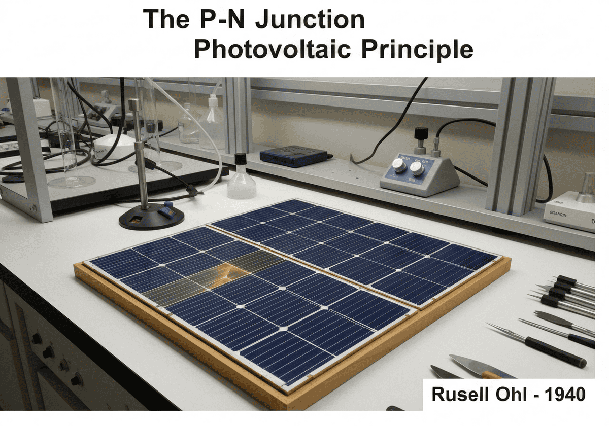
A solar cell’s core is a p-n junction, an interface between p-type and n-type semiconductor materials. This junction creates a built-in electric field in a depletion region. When photons with sufficient energy strike the semiconductor, they create electron-hole pairs. The electric field separates these charge carriers, driving electrons to the n-side and holes to the p-side, generating a voltage.
The P-N Junction Photovoltaic Principle
- Russell Ohl
The p-n junction is the fundamental building block of most solar cells. It is formed by joining a p-type semiconductor, which has an excess of holes (positive charge carriers), with an n-type semiconductor, which has an excess of electrons (negative charge carriers). This is typically achieved by doping a single semiconductor crystal, like silicon, with different impurities on each side.
At the interface, electrons from the n-side diffuse into the p-side, and holes from the p-side diffuse into the n-side. This diffusion process doesn’t continue indefinitely. As electrons and holes cross the junction, they recombine, leaving behind ionized donor atoms on the n-side and ionized acceptor atoms on the p-side. This creates a region depleted of free charge carriers, known as the depletion region or space charge region. The fixed, ionized atoms in this region establish a strong, static electric field pointing from the n-side to the p-side.
This built-in electric field is crucial for the photovoltaic effect. When a photon with energy greater than the semiconductor’s bandgap energy ([latex]E_g[/latex]) is absorbed, it excites an electron from the valence band to the conduction band, creating an electron-hole pair. If this pair is generated within the depletion region or close enough to diffuse into it, the electric field acts on them. The field sweeps the electron towards the n-side and the hole towards the p-side. This separation of charge prevents immediate recombination and creates an accumulation of positive charge on the p-side and negative charge on the n-side. This charge separation across the device results in a photovoltage, which can drive a current through an external circuit, thus converting light energy into electrical energy.
Tipo
Disruption
Utilización
Precursors
- discovery of the photoelectric effect by heinrich hertz (1887)
- einstein’s explanation of the photoelectric effect (1905)
- development of semiconductor physics and doping techniques
- discovery of rectification at a metal-semiconductor contact (1874)
Aplicaciones
- photovoltaic solar panels
- photodiodes
- light-emitting diodes (leds)
- semiconductor transistors
Patentes:
- US2402662A
Potential Innovations Ideas
Membresía obligatoria de Professionals (100% free)
Debes ser miembro de Professionals (100% free) para acceder a este contenido.
DISPONIBLE PARA NUEVOS RETOS
Mechanical Engineer, Project, Process Engineering or R&D Manager
Disponible para un nuevo desafío a corto plazo.
Contáctame en LinkedIn
Plastic metal electronics integration, Design-to-cost, GMP, Ergonomics, Medium to high-volume devices & consumables, Lean Manufacturing, Regulated industries, CE & FDA, CAD, Solidworks, Lean Sigma Black Belt, medical ISO 13485
Estamos buscando un nuevo patrocinador
¿Su empresa o institución se dedica a la técnica, la ciencia o la investigación?
> Envíanos un mensaje <
Recibe todos los artículos nuevos
Gratuito, sin spam, correo electrónico no distribuido ni revendido.
o puedes obtener tu membresía completa -gratis- para acceder a todo el contenido restringido >aquí<
Historical Context
The P-N Junction Photovoltaic Principle
(if date is unknown or not relevant, e.g. "fluid mechanics", a rounded estimation of its notable emergence is provided)
Related Invention, Innovation & Technical Principles