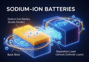
钠离子电池最新出版物和专利
This week: lithium-sulfur battery, positive electrode, sulfide-based composite, solid electrolyte, slurry, all-solid-state battery, positive electrode, sulfide-based electrolyte, Electrochemical, Carbon Capture,
This week: lithium-sulfur battery, positive electrode, sulfide-based composite, solid electrolyte, slurry, all-solid-state battery, positive electrode, sulfide-based electrolyte, Electrochemical, Carbon Capture,

Our smiling view on today’s news: Researchers have uncovered evidence of a prehistoric organism that does not fit into any
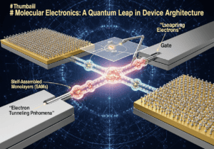
This week: polymer analysis, nanopore sensor, machine learning, measurement signal, Nitride, semiconductor, electron transport, gate electrode, photoelectric conversion, perovskite structure,
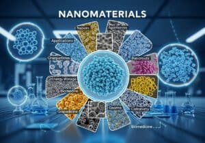
This week: nanocoating, encapsulation, metal-polyphenol nanoparticles, cellular integrity, quantum dots, light-emitting devices, organic ligands, hydrocarbon groups, cerium oxide, zirconium dioxide,

This week: TFT, color filter, liquid crystal display, organic resin film, Quantum propulsion, Bose-Einstein Condensate, Magnetic Coherence Focuser, Adaptive Energy