» 碳纳米管场效应晶体管(CNTFET)

碳纳米管场效应晶体管(CNTFET)

1998
  • Sumio Iijima
  • Cees Dekker
  • Phaedon Avouris
碳纳米管场效应晶体管在实验室环境中的材料科学应用。

(generate image for illustration only)

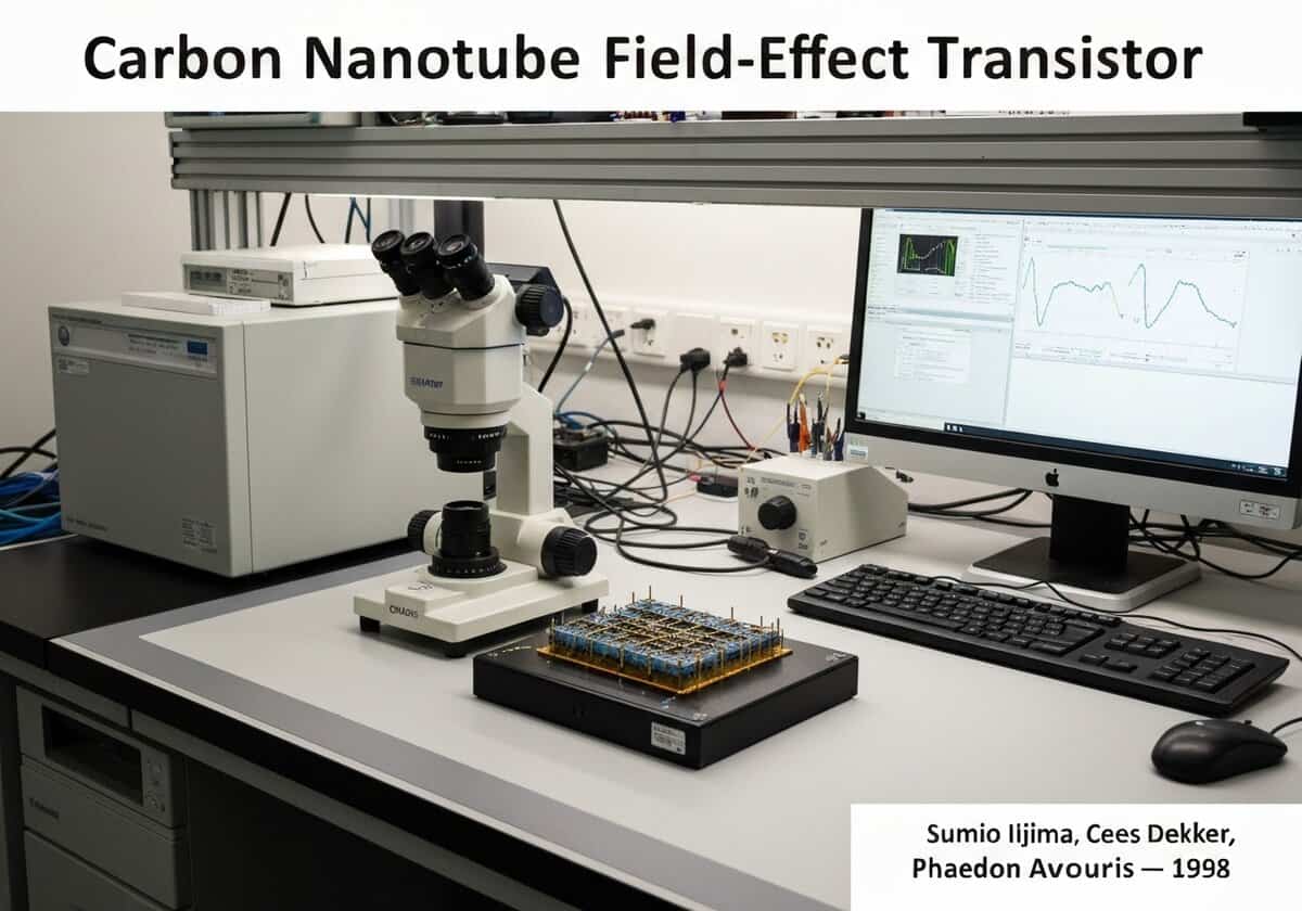
A Carbon Nanotube Field-Effect 晶体管 (CNTFET) utilizes a single carbon nanotube (CNT) or an array of CNTs as the channel material instead of bulk silicon. Depending on its chirality (the arrangement of its graphene lattice), a CNT can be either metallic or semiconducting, making it a versatile building block for nanoelectronic devices with superior performance potential.

A CNTFET operates on the same principle as a conventional MOSFET. It has a source, a drain, and a gate terminal. The key difference is the channel, which is formed by one or more carbon nanotubes. When a voltage is applied to the gate, it creates an electric field that modulates the conductivity of the semiconducting CNT, turning the flow of current between the source and drain ‘on’ or ‘off’. The exceptional properties of CNTs make them highly attractive for this application. They exhibit extremely high carrier mobility, meaning electrons can travel through them with very little scattering, which translates to faster switching speeds and higher current-carrying capacity. Their one-dimensional structure provides excellent electrostatic control by the gate, reducing short-channel effects that plague scaled-down silicon transistors.

然而,CNTFET 的广泛商业化面临诸多挑战。其中最大的障碍是 CNT 的合成。典型的合成方法会产生金属纳米管和半导体纳米管的混合物。金属纳米管会造成短路,阻止晶体管完全关闭,并导致高漏电。大规模分离 100% 纯度的这些纳米管既困难又昂贵。另一个挑战是将 CNT 以精确的排列和密度放置在晶圆上。最后,在纳米管末端建立低电阻电接触并非易事,这可能会限制器件的整体性能。

Despite these issues, research has made significant progress. Techniques have been developed to selectively remove metallic CNTs or to convert them into semiconducting ones. Demonstrations of complex circuits, including a 16-bit microprocessor, have been built using CNTFETs, proving the viability of the technology. Their unique properties also make them ideal for novel applications like highly sensitive biosensors, where the CNT’s conductance changes dramatically upon the attachment of a target molecule, and for flexible electronics due to their inherent mechanical strength and flexibility.

UNESCO Nomenclature: 3313
- 材料科学

类型

物理设备

中断

实质性

使用方法

新兴技术

前体

  • 场效应晶体管(FET)的发明
  • 富勒烯的发现
  • 碳纳米管的发现和合成
  • 半导体制造技术(光刻、沉积)的发展

应用

  • 高频电子器件
  • 化学和生物传感器
  • 柔性透明电子产品
  • 未来逻辑电路中硅的潜在替代品

专利:

  • US6835601B2
  • US7015501B2

潜在的创新想法

级别需要会员

您必须是!!等级!!会员才能访问此内容。

立即加入

已经是会员? 在此登录
Related to: CNTFET, carbon nanotube, field-effect transistor, carrier mobility, chirality, nanoelectronics, post-silicon technology, flexible electronics.

发表回复

您的邮箱地址不会被公开。 必填项已用 * 标注

迎接新挑战
机械工程师、项目、工艺工程师或研发经理
有效的产品开发

可在短时间内接受新的挑战。
通过 LinkedIn 联系我
塑料金属电子集成、成本设计、GMP、人体工程学、中高容量设备和耗材、精益制造、受监管行业、CE 和 FDA、CAD、Solidworks、精益西格玛黑带、医疗 ISO 13485

我们正在寻找新的赞助商


您的公司或机构从事技术、科学或研究吗?
> 给我们发送消息 <

接收所有新文章
免费,无垃圾邮件,电子邮件不分发也不转售

或者您可以免费获得完整会员资格以访问所有受限制的内容>这里<

历史背景

(如果日期不详或不相关,例如 "流体力学",则对其显著出现的时间作了四舍五入的估计)。

相关发明、创新和技术原理

滚动至顶部

你可能还喜欢