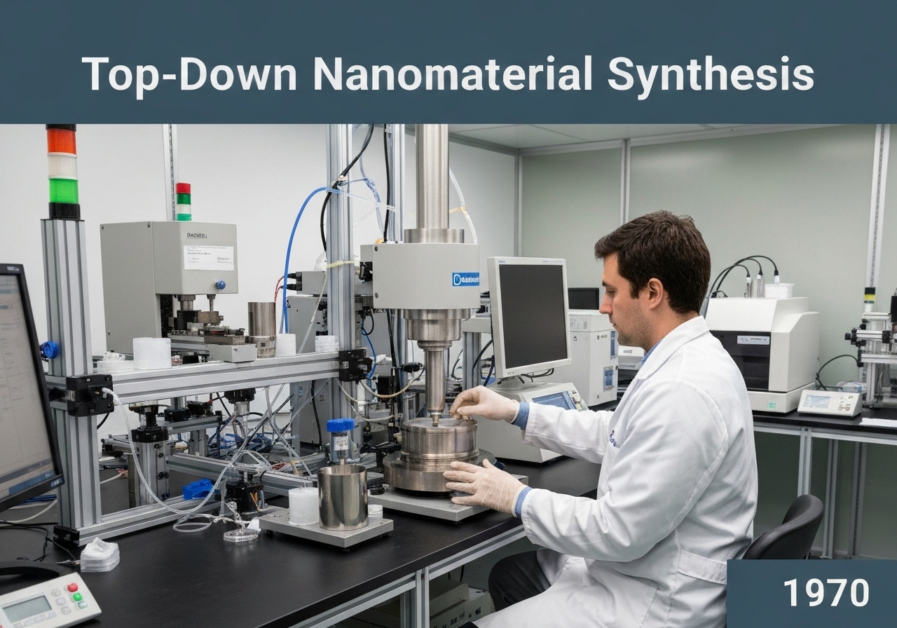
탑다운 합성법은 더 큰 벌크 재료에서 시작하여 이를 나노 크기로 분해하거나 패턴화하여 나노 재료를 만드는 방법입니다. 주요 기술로는 볼 밀링과 같은 기계적 방법과 포토리소그래피, 전자빔 리소그래피, 나노임프린트 리소그래피와 같은 리소그래피 방법이 있습니다. 이러한 방법들은 구조화된 표면이나 집적 회로를 만드는 데 자주 사용되지만, 표면 결함이 발생할 수 있다는 단점이 있습니다.


탑다운 나노소재 합성
(날짜를 알 수 없거나 관련이 없는 경우, 예를 들어 "유체역학"의 경우, 주목할 만한 등장 시기를 대략적으로 추정하여 제공합니다.)